

In this article, we will introduce the basic concepts of the MOSFET, with focus on its two main forms: the NMOS transistor and the PMOS transistor. We will also discuss briefly the manufacturing process, the mathematical models and the two main applications of NMOS and PMOS: amplifiers and switches.
The article Ultimate Guide to: Electronic Circuit, presents the concepts of passive and active components, as well as the basics of transistors. However, we focused on the bipolar transistor, which is widely used, but far from the only one in electronics. In this article, we will discuss the Metal-Oxide Field Effect Transistors, or MOSFET for short. These transistors are widely applied in mixed-signal instrumentation, ASICs and switched-mode power supplies. Understanding NMOS and PMOS transistors, as well as where they are applied and how to implement them, is fundamental, as they have become the main choice of transistor for almost any application. They provide very large input impedance, fast switching capabilities, small ON resistance, and very small footprint, which is perfect for high density designs.
In electronic terms, the working principle of a transistor is very simple: it has three main terminals, and the current flowing through one of its terminals can be controlled by the voltage between the other two terminals. In the case of a MOSFET, the voltage between the gate and the source ports controls the current flowing through the drain. The relationship between the drain current (ID) and the gate-to-source voltage (VGS) is highly non-linear, and it is divided in three operation regions. Each region has its own conditions, properties and equations, as described in the table below:
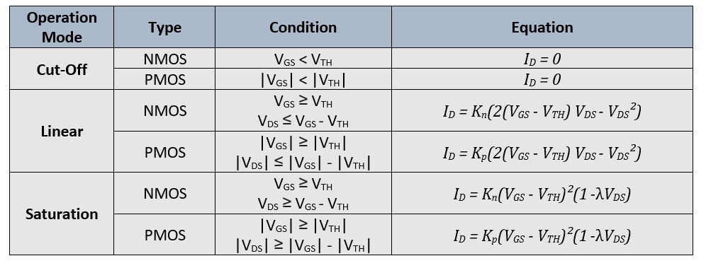
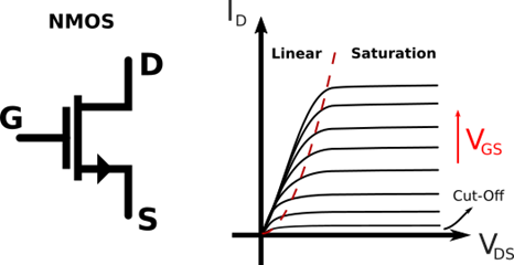
Figure 1: NMOS symbol, characteristic curve and operation modes
In practical terms, the operation modes describe how the drain current (ID) reacts to a variation in the drain to source voltage (VDS), and are key to understand the MOSFET applications. In the cut-off region the transistor acts as an open-circuit between drain and source, in the linear region the relation between VDS and ID is almost ohmic, and in the saturation mode the current is – ideally – independent on VDS. The channel-length modulation effect prevents the current to be completely independent of VDS, so the λ term describes how the current changes with VDS during saturation. The constants Kn and Kp depend on the MOSFET material (oxide capacitance and charge mobility) and geometry (channel width W and length L). When developing a microelectronics circuit, the designer can use the W and L values to control the current equation. In circuit design, the gate-to-source voltage VGS is used to control the operation mode of the transistor.

There are two types of MOSFETs: the NMOS and the PMOS. The difference between them is the construction: NMOS uses N-type doped semiconductors as source and drain and P-type as the substrate, whereas the PMOS is the opposite. This has several implications in the transistor functionality (Table 1). The most evident one is the drain current direction and the voltages polarity: the threshold voltage VTH, the VGS and the VDS are negative. Secondly, the charge carriers are not the same: NMOS uses electrons and PMOS uses holes as majority carriers. This greatly affects the K constant, resulting in several differences:
The NMOS is used more often due to its advantages, however many applications require the polarization characteristics of the PMOS. Also, in analog and digital microelectronics both NMOS and PMOS are widely used. Particularly, one of the most popular MOS structures applies both: the CMOS (complementary MOS). This structure (Figure 2) acts as a digital inverter: when the voltage VG is low, the NMOS turns off and the PMOS turns on, creating a low impedance path from the output to VCC, and when VG is high the NMOS turns on and the PMOS turns off, resulting in a low impedance path to ground. This ensures that the output pin is always connected to a stable and well defined voltage, which is essential for digital systems. Of course, both NMOS and PMOS should be designed to operate symmetrically.
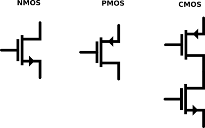
Figure 2: The NMOS symbol, PMOS symbol and CMOS symbol
Although the transistor operation can be described by the gate, drain and source, the MOSFET is actually a 4-pin device. The fourth port is called body, and it is connected to the substrate of the transistor. If the voltage between the body and the source is different from zero, the transistor will suffer from the body-effect. The body-effect changes the threshold voltage VT and can be used to dynamically modify the properties of the transistor. However, it is usually considered an undesired effect, that occurs when the body node is not directly connected to the source voltage. For simplicity, every equation in this article considers VBS = 0 V, so the body-effect is nulled.
Figure 3: NMOS without and with body effect.
MOS transistors are built on top of silicon wafers. This process uses semiconductor doping and oxide growth to create N-type, P-type and insulating regions in a layer-by-layer fashion. Geometric shapes are obtained via photolithography and chemical etching. A simplified illustration of the NMOS and PMOS cross-section can be seen in Figure 4.
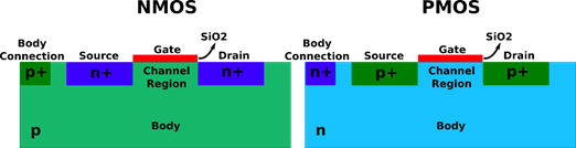
Figure 4: NMOS and PMOS cross-sections
The drain and source regions are strongly doped with N-dopants (NMOS) or P-dopants (PMOS), and the substrate is doped with the opposite type (P-type for NMOS and N-type for PMOS). This alternation results in a depletion region that blocks any current between drain and source, which explains the cut-off region. The gate is connected to a thin layer of silicon dioxide, that insulates the gate connection from the substrate. When voltage is applied to the gate, the electric field attracts minority carriers to the region below the SiO2 layer. This is the “FET” (Field-Effect Transistor) part of the MOSFET. When enough charge is accumulated in that region, the minority carriers become the majority carriers, forming a channel with the same type as the drain and source (Figure 5). The gate-to-source voltage that results in channel inversion is the threshold voltage VTH. This is why NMOS require positive voltages (to attract electrons) and PMOS require negative voltages (to attract holes) for channel formation.
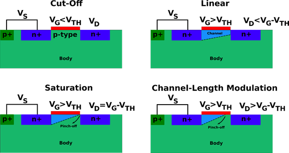
Figure 5: Channel formation and pinch-off in a NMOS transistor.
The channel presents ohmic resistance for a fixed VGS (linear operation mode) as long as VDS remains smaller than the VGS – VTH. After that, the charge concentration near the drain is nulled, and the channel becomes “pinched”. This is called channel pinch-off, and marks the division between the saturation and linear regions. As VDS increases, the pinch point moves and the effective length of the channel reduces, which results in the channel-length modulation effect discussed previously.
It is difficult to cover every application of the NMOS and PMOS, as they can be used as active loads, voltage-controlled resistors, transimpedance amplifiers, current mirrors and even capacitors and diodes. Thus, we will focus on the most popular applications: voltage amplifiers and switches. However, the same reasoning used here can be applied to other cases.
Both NMOS and PMOS can be considered “voltage to current” converters, so one can design a voltage amplifier by simply adding a resistive load to the current output. However, in order to act as a proper current source, the drain current must be independent of the drain voltage (in other words, the output impedance should be really high). Therefore, to be used as a voltage amplifier, the MOSFET should operate inside the saturation region. Also, due to the highly non-linear nature of the current equations, the input signal should be kept small, to prevent non-linear effects. Circuit linearization techniques are available in the literature.
There are three main types of MOSFET amplifiers: the common-source, the common-drain and the common-gate. The difference between them is the role of each pin.
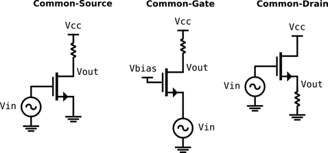
Figure 6: Common-Source, Common-Drain and Common-Gate Amplifiers using NMOS.
The circuit design and analysis of these amplifiers can be done in three major steps:
A good switch can be defined by two characteristics: it provides a very large impedance if off and a very small impedance if on. If it fails to open the circuit, leakage currents will pass through and the signal path will become uncontrolled. If it fails to close, voltage drops will attenuate the signal and power losses will increase. MOSFETS are very good in both properties, as they provide very large impedance paths in the cut-off region, and very small series resistance in the linear region. Also, the command signal is isolated from the signal path, which simplifies significantly the control circuit. The low on resistance and high gate impedance are extremely desirable in switched-mode power converters, as they increase the efficiency significantly. Moreover, the small footprint of MOS switches escalates tremendously the density of logic ports inside one chip, which was fundamental for the digital boom in modern technology.
Both NMOS and PMOS transistors can be used as switches, and the application depends on the control signal and the current direction. In microelectronics applications, where the MOSFET dimensions can be modified, it is important to design the transistor to obtain a very low resistance point in the closed state, which can be done by modifying the W and L and the technology. Also, the parasitic capacitances should be minimized to prevent crosstalk through the transistor when in open state. Peak voltage, charge injection, maximum current and switching time are examples of parameters that should also be controlled. For applications using discrete MOSFETs, which is the case of most switched-mode power converters, the transistor switch should be selected considering all the above requirements, as well as heat dissipation and gate driving. There are several topologies of MOSFET switches. Figure 7 shows three different implementations: a simple NMOS switch, a transmission gate that allows bidirectional current and a CMOS digital inverter, that can be seen as a complementary switch.
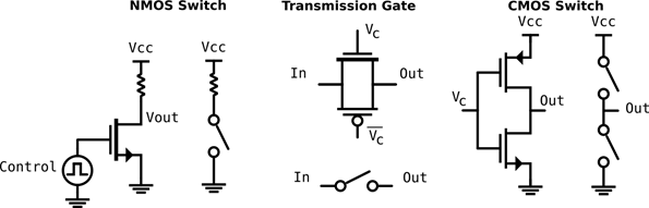
Figure 7: NMOS switch, a transmission gate for bilateral switching and the CMOS inverter.
Looking for prices?
Calculate your die per wafer (DPW)
Start your SoC design today, click here