

There are numerous steps that are involved in the design of digital (or mixed signal) circuits starting from system specifications right till the chip is manufactured. One of these steps is a process of transforming a functionally described circuit (normally in netlist) into physical layout at the lowest level (normally defined in GDSII). This process is normally referred to as Physical Design (PD) in the chip manufacturing flow.
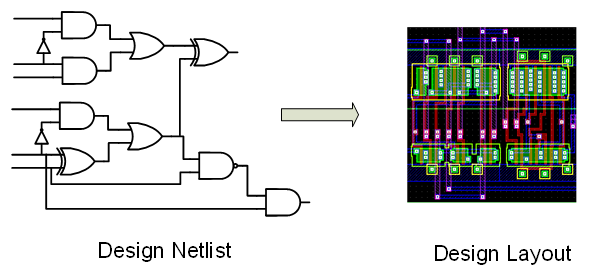
Figure 1: Netlist to Layout
This physical layout describes what cells to be used (normally defined in technology library), position of cells and routes for the interconnections between them. The physical design process makes sure that the final chip does fulfill (or improve) numerous physical constraints of the final product such as area, power, temperature of the die. The process does not affect any functionality of the design itself. The physical design process can be further sub categorized into various steps:
The very first step in physical design process is to do the partitioning of the design into smaller parts, normally called macros. This step is optional for very small designs where complete chip can be laid out in one go. However, in most of the designs, the partitioning of design is of paramount importance and affect the overall architecture of the design too. The goal is to divide the design into functional blocks so that gates that belong to same function are located close to each other. This allows the smaller macros to be laid out independently to each other. However, during this portioning one must minimize the number of connections between these macros. An example of portioning of design into three partitions can be viewed below
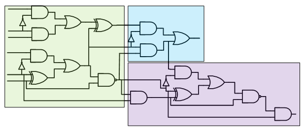
Figure 2: Partitioning Example
Floor planning of an ASIC/circuit should be viewed as floor planning activity of an house. Once the design has been partitioned into macros (like rooms in our house), the next step is to place these macros in an optimized way. Just as we would like to have some kind of flow in our living rooms, the goal is to place structure with connections close together. The floor planning does require the physical designers to be aware of the data and control flow in the chip so they can optimize the locations. This also requires designers to be aware of area restrictions, number of signals to be routed between different macros and speed of those signals. The floor planning can be viewed as iterative process to achieve best performance for the design in terms of area and power. An example of a design with a floorplan is shown below where Macros are placed w.r.t data flow and IO placements.
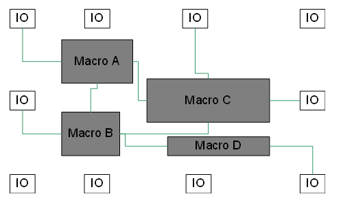
Figure 3: Example floorplan of a circuit
Once all the floorplan is completed and placement of the cells is finished on the silicon area, we have to interconnect all the pins (inputs/outputs of the macros) according to the specifications. This process is called Routing.
In a typical circuit, there are millions of wires that needs to be connected. They do not only need to be connected but must fulfill a lot of design constraints in terms of delay of the wires, cross talk, max transition times etc. Routing is done on a number of metal layers but adding metal layers would increase the overall cost of the die. The goal is also to minimize the total wire length and area of the die.
Routing is normally considered with an assumption that layout area is a grid of equal squares. A connection is made when a cell defined as S (Source) can be connected to a cell T (Target). In picture below, “black” boxes represent already used part of the grid. To connect S to T, an example path is shown in green.
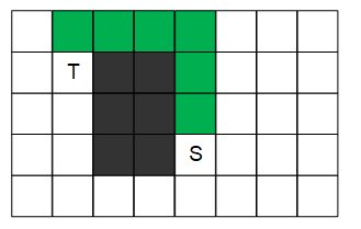
Figure 4: Routing Grid
Wires can only traverse North, South, East, or West. When several layers are used for routing, each layer is considered as a separate grid. However, signals can transverse up and down as well.
Normally routing process is divided into two steps.
Clock is the main component for the sequential part of the digital design where it acts as synchronizer for all flip flops. The performance of the design quite simply depends on the speed of the clock. The faster the clock, the faster the ASIC can do processing. However, one cannot increase the speed of the clock beyond a certain limit (constrained by power or delays of the wires). Normal signals routing principles do not apply to clock because it is fundamentally different. They have much larger fanouts than normal signal and have very high toggle rate as compared to normal signals.
The goal of CTS is to distribute the clock to all the flops (residing in all corners of the ASIC) with minimum skew and minimum jitter. The skew is handled mainly by making sure that all leaf cells (FFs) receive the clock at roughly the same time. This will make sure that delay of those routes will be roughly the same. However, the designer must cater for the delay changes due to incur because of process, temperature, and voltage variations.
Normally the delays to different functional blocks are aligned by using special routing such as clock tree. A typical clock tree is shown in figure below where route from clock source to all FFs are aligned. Typically, the route is driven by clock tree cells and clock buffers on the way to make sure they reach end points with a good SNR (Signal to noise ratio).
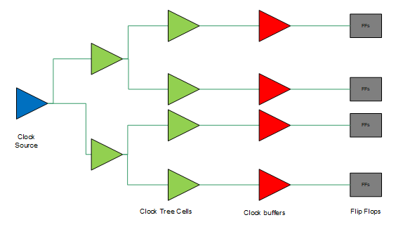
Figure 5: Clock Tree
There are many other clock tree networks (such as H-type, X-type) that can be deployed for certain use cases and certain floorplans. However, concepts remain the same to minimize the skew and jitter during the distribution.
The VDD (power) and VSS (ground) signals have more similarities to clock routing as they need to be distributed to virtually all the cells of the design (sequential as well as combinatorial). However, the main requirement for power signal routing is not to minimize the skews or jitter but to make sure that enough current is provided when required.
Power and ground nets are routed in metal layers due to its very low resistivity and normally kept on same metal layers throughout the ASICs.
The majority of digital designs constitute sequential elements. These elements (such as a DFF) require a certain behavior in terms of data and clock reaching to the pins of the FF. One of the most important aspect during the chip manufacturing is timing closure. Timing closure can be viewed as timing verification of the digital circuit.
Timing closure process makes sure that data arrives a certain time earlier than the clock edge fulfilling the setup time requirement of the FF. Similarly, it will also make sure to check that data is stable some time after the clock edge fulfilling the hold timing requirement of the FF.
As we know that delay of the wire does change across temperature as well as voltage level and also the process corner of the die, the goal of the timing closure analysis is to make sure these, setup and hold requirements are fulfilled for all different PVT corners.
The advantage of using STA rather than timing driven gate level simulation is that gate level simulations are much slower and would require an exhaustive list to check every constrained timing path. With STA process, one can test all the paths without generation of any vectors.
One of very important steps in physical verification is called DRC. The step is important since the complexity of physical layouts have been increasing rapidly. A typical SoC design will contain millions of transistors and those will be laid out in billions of rectangular shape polygons. Now there can be many issues while laying out these rectangular polygons such as two wires are too narrow to each other, or width of the wires are not wide enough to support the required current/load on those wires. All these issues can result in failure of the device and thus must be verified before the actual fabrication process starts.
So, in this process, the physical designer specifies some general rules for example, the width of the wire and distance between the two wires. And then the tool makes sure that these rules are always honored.
There are few things that must be done to make sure that all physical layout and design fulfills all the requirements before it can be signed off for fabrication. Some of these extra steps are:


