

System in Package (SiP) is a method used for bundling multiple integrated circuits (ICs) and passive components into a single package, under which they all work together. This contrasts to a System on Chip (SoC), whereas the functions on those chips are integrated into the same die.
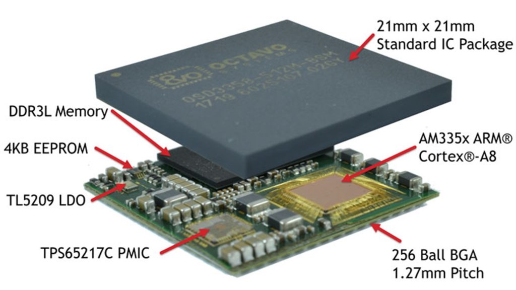
Figure 1: Example of a SiP (source: Octavo Systems)
Silicon dies containing different circuits based on various process nodes (CMOS, SiGe, BiCMOS) may be stacked vertically or side by side on a substrate. The package consists of an internal wiring that connects all the dies together into a functional system. Wire bonding or bumping technologies are typically used in system in package solutions.
A System in Package is similar to a System-on-a-Chip, but it is less tightly integrated, and it is not made using a single semiconductor die. A common SiP solution may make use of multiple packaging technologies, such as flip chip, wire bonding, wafer-level packaging, etc.
The variable number of integrated circuits and other components enclosed in system in package is in theory unlimited, therefore, engineers can essentially and integrate an entire system into a single package.
In the 1980s, SiP were available in the form of multi-chip modules. Instead of putting chips on a printed circuit board, they can lower cost and/or shorten the distances that electrical signals need to travel by combining the chips into a single package, with connections historically being made through wire bonds.
The main driving force behind the development and use of semiconductors has been integration. Starting with SSI (Small Scale Integration – few transistors on a single chip), the industry has moved to MSI (Medium Scale Integration – hundreds of transistors on a single chip), LSI (Large Scale Integration – tens of thousands of transistors on a single chip), ULSI (Ultra Large Scale Integration – more than one million transistors on a single chip), VLSI (Very Large Scale Integration – billions of transistors on a single chip) and finally WSI (Wafer Scale Integration – a whole wafer becomes a single super chip).
All of these were physical integration metrics, not taking into account the functional integration needed. As such, several terms popped up to fill in the gaps, like ASICs (Application Specific Integrated Circuits) and SoCs (System-on-Chip), which shifted the focus to more system integration.
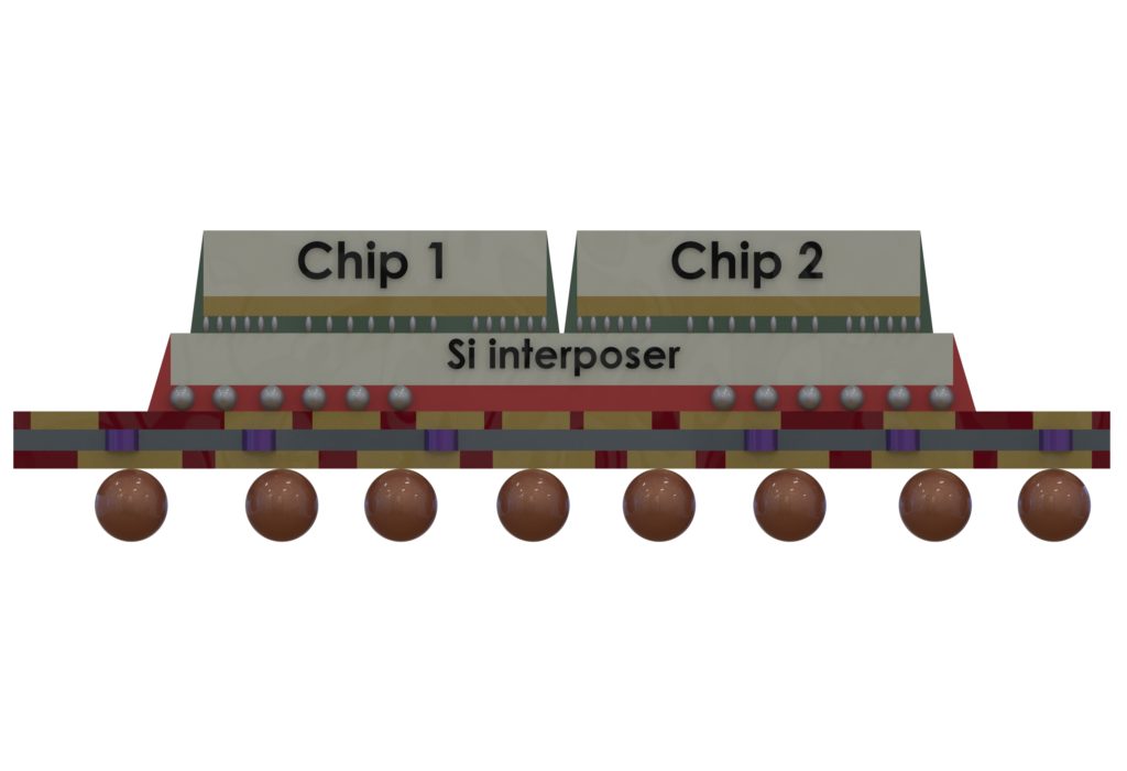
Figure 2: Example of a SiP – Inside View
As for the original need for SiPs, we need not look further than the microprocessor. The requirements for the development and production of microprocessors are very different from those of analog circuits, power management devices or memory devices. This has led to the obvious increased integration at the system level.
Even though the term SiP is relatively new, in practice SiPs have been a part of the semiconductor industry for a long time.
In the 1970s it was in the form of discretionary wiring, multi-chip modules (MCMs) and hybrid integrated circuits (HICs).
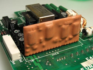
Figure 3: Example of a HIC
In the 1990s it was used as a solution for Intel’s Pentium Pro3 integrated processor and cache. Nowadays, SiPs have been turned into a solution for integrating multiple chips into a single package to reduce space and cost.
The main difference between SiPs and SoCs is that the SoC incorporates every single component needed on the same die, whereas the SiP approach takes heterogeneous components and connects them into one or more chip carrier packages.
For example, an SoC would integrate the CPU, GPU, memory interfaces, HDD and USB connectivity, RAM/ROM and/or their controllers on a single silicon, which then gets packaged into a single chip. In contrast, an equivalent SiP would take the separate dies from different process nodes (CMOS, SiGe, High Power), connect and combine them into a single package onto a single substrate (PCB). With this in mind, it is easy to see that SiPs have a lower degree of integration when compared to similar SoCs, and, as a result, adoption of SiPs has been slow.
More recently though, advancements made in 2.5D and 3D ICs, flip chip technology, and package on package technology have shone a new light on the possibilities offered by using a SiP.
There are a couple of major elements that drive this current trend of replacing SoCs with SiPs:
Apart from the factors mentioned above, SiPs offer even more advantages as follows:
For a complete view though, we have to acknowledge that SiPs can have some drawbacks, as well. Here are some major disadvantages that need to be taken into consideration before picking SiP as the design philosophy:
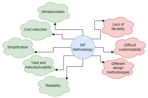
Figure 4: Pros and Cons of using System in Package
One could summaries SiPs to consist of a substrate on which several chips are combined with passive components to create a complete functional standalone package, to which only a few components need to be externally attached to create the desired product. Due to the size reductions and tight integration that result from this, SiPs are very popular in space constrained devices, such as MP3 players and smartphones. On the other hand, if only one component is defective, the whole system becomes non-functional, leading to a decreased manufacturing yield.
In spite of this, the main driving force behind the push for more development and production of SiPs is the early wearable, mobile devices and IoT devices market. Here, demand is still manageable under current SiP constraints, with lower numbers than the established enterprise and consumer SoC market.
As the IoT era comes more and more into the picture, constant development and research helps bring SiPs closer to SoCs, with costs lowering, smaller volume requirements and initial investments, and with a positive trend in system simplification. Also, the push to create larger and larger monolithic SoCs is starting to hit the wall of design verification and manufacturability, as having a bigger die leads to a greater failure chance and thus a more substantial loss of silicon wafer.
When looking at the IP side, SiPs are a great future alternative to SoC, due to the fact that they can integrate the latest standards and protocols without a constantly lengthier and more expensive redesign phase. Plus, SiP methodology allows for faster and more energy efficient communication and power delivery, which is another encouraging factor to take into consideration when looking at the long term prospect of SiP adoption and applications.
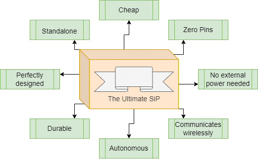
Figure 5: The Ultimate System in Package Properties
But what does the ultimate SiP look like? In theory, it should be a standalone component with zero connections to the outside. It is a custom component that perfectly suits the job it was meant to do, all the while requiring no external physical connections for communications or power. It should be able to generate or harvest its own power, function autonomously, and communicate wirelessly with an information system. Also, it should be relatively cheap and resistant to the elements, allowing it to function in most weather conditions and to be cheaply exchanged in the case of failure.
With demand for more and more simplification and system-level integration, the components of today will become the SiP-ready components of tomorrow, while the SiPs of today will become Sub-System in Packages (SSiPs). SiP-ready components and SSiPs will then be integrated into larger SiPs as system integration drives SiP technology ever closer to the final goal: the ultimate SiP.
Get an indicative packaging cost range, then a detailed breakdown by email.


