Collaboration aims to accelerate Europe’s adoption of chiplets and advanced 2.5D and 3D chip packaging solutions
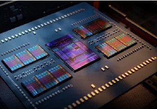
December 15, 2025 — Avnet ASIC, a leading provider of ASIC and SoC turnkey solutions, a division of Avnet (NASDAQ: AVT) and a TSMC VCA, together with Bar-Ilan University, announced a strategic collaboration to establish an Advanced Chiplet Innovation Center, scheduled to open in 2026. Located within Avnet ASIC’s facility, the center will focus on developing next-generation 2.5D and 3D integration solutions based on TSMC’s advanced technology nodes, tailored to the rapidly growing European ASIC market.
The partnership brings together Avnet ASIC’s proven expertise in ASIC design, physical implementation, and advanced packaging, with Bar-Ilan University’s EnICS Institute, a leading academic research group in advanced semiconductor architecture, research and development. By combining industry experience and academic innovation, the center aims to create unique design approaches and provide a practical platform for translating research into deployable advanced chiplet packaging solutions.
Meeting Europe’s Growing Demand for Chiplets and Advanced Integration
Europe’s semiconductor ecosystem is expanding through both public and private initiatives, creating increasing demand for advanced chip packaging capabilities. European fabless companies, in particular, require chiplet architectures, 2.5D interposers, and 3D integration solutions to meet modern performance, power, and form-factor requirements.
The Advanced Chiplet Innovation Center will offer a collaborative environment where Avnet engineers and Bar-Ilan researchers work side by side to develop, evaluate, and refine advanced heterogeneous integration technologies under Avnet’s technical umbrella. The platform leverages TSMC’s leading-edge process nodes as its technical foundation, ensuring that designs are compatible with global high-performance manufacturing standards while remaining flexible for European customer requirements.
A New Model for Industry–Academic Collaboration
Operating as a physical hub within Avnet ASIC’s development facility, the center will focus on integrated 2.5D and 3D chiplet packaging solutions on the most advanced TSMC technologies. Workstreams include electrical and mechanical co-design, simulation and optimization, power integrity, thermal modeling, and signal integrity, as well as verification methodologies for chiplet-based architectures.
The collaboration also enables Bar-Ilan University to channel cutting-edge academic research directly into industry, providing a unified environment where innovation and practical engineering converge. This approach helps European companies accelerate innovation while mitigating risk, bridging the gap between academic discovery and industrial deployment.
Yulia Milshtein, GM and Head of Business of Avnet ASIC, said: “European companies are increasingly seeking local advanced packaging solutions to meet complex system integration requirements. By combining Bar-Ilan University’s research capabilities with our engineering and manufacturing expertise, we are creating a platform that helps the European fabless community bring complex architectures to market faster and more reliably.”
Prof. Alexander Fish, Founder and Co-director of the EnICS Labs Institute at Bar-Ilan University, added: “This collaboration allows our researchers to translate cutting-edge academic work into real-world advanced implementations. Together with Avnet ASIC, we strengthen Europe’s semiconductor capabilities and provide a practical path for innovation.”
About Avnet ASIC
Avnet ASIC is a division of Avnet, a global technology distributor with a track record of supporting semiconductor innovation. Avnet ASIC is a TSMC VCA (Value Chain Aggregator) and provides turnkey ASIC and SoC solutions down to 2nm, partnering with TSMC, Outsourced Semiconductor Assembly and Test companies (OSATs), and leading IP and CAD vendors to deliver services from specification to mass production for startups, OEMs, and international companies.
About the EnICS Lab at Bar-Ilan University
Bar-Ilan University’s Emerging Nanoscaled Integrated Circuits & Systems (EnICS) Institute conducts research in SoC architecture and design, high-speed digital ICs, energy-efficient embedded memories, hardware security, advanced analog circuits, and other emerging technologies. With a track record of more than 50 successful tape-outs in advanced process nodes, the Institute collaborates with industry to translate cutting-edge academic research into real-world semiconductor applications.
For more information:
Avnet ASIC: https://www.avnet-asic.com
EnICS Lab: https://enicslabs.com
Images can be downloaded here.