

Integrating photonic devices into reliable, scalable modules and systems is still one of the industry’s most complex challenges. Yet that same complexity is also creating value, with the photonics packaging market projected to reach $14.4 billion by 2031.
Today’s insights highlight key trends explored in Yole Group’s latest report, Photonics Packaging 2026, the central focus of this article. This report delivers a comprehensive analysis of packaging technologies, integration strategies, and industrial challenges shaping the photonics ecosystem, while uncovering new opportunities across applications and markets.
Authored by Eric Mounier, PhD, Chief Analyst, Photonics and Raphaël Mermet-Lyaudoz, PhD, Technology & Market Analyst, Photonics and Display at Yole Group, this article is part of Yole Group’s broader portfolio of photonics market and technology reports, including Optical Transceivers for Datacom and Telecom 2026, Silicon Photonics 2026, Co-Packaged Optics for Data Centers 2026, and more.
Yole Group continuously analyzes the photonics ecosystem to address AI challenges and highlight key innovations shaping the market. Leveraging strong expertise in photonics and AI dynamics, its portfolio helps stakeholders navigate this transition and make informed strategic decisions.
Enjoy this new strategic insight, perfect with your coffee.
At its core, photonics packaging is a module-level assembly exercise. It involves bringing together a broad mix of components to create a complete optical engine, including laser dies, fiber-array units, silicon photonics chips, prisms, and photodiode arrays. This is the type of architecture commonly found in today’s optical transceivers, which still account for the largest share of the market. That market, however, is evolving. Optical transceivers are shifting from hybrid integration, where source dies are flip-chipped onto silicon photonics devices, toward heterogeneous integration, in which dies are processed directly on the silicon photonics chip after bonding. A deeper disruption, though, is coming from co-packaged optics (CPO), where photonic integrated circuits (PICs) are stacked with electronic integrated circuits (EICs).
This transition plays directly into the strengths of advanced semiconductor foundries. Companies such as TSMC and ASE are well-positioned to play a pivotal role, not only as manufacturing leaders but also as potential standards-setters. And standardization will be critical if the industry is to move from innovation to large-scale deployment. However, several architectural questions remain unresolved: Should the industry favor PIC-on-EIC or EIC-on-PIC, as in TSMC’s current approach? Will hybrid bonding prevail over fan-out micro-bumping? And on the optical side, which coupling strategy will dominate: V-groove, edge couplers, or grating couplers? TSMC’s COUPE platform, for example, is being promoted with both edge and surface/grating approaches under consideration.
For now, no single option clearly stands above the rest. The outcome will likely depend less on any one technology’s intrinsic superiority than on broader system-level requirements. Will future systems rely on wide spectral-band data exchange? Will alignment accuracy become the main bottleneck? These are the questions still facing the industry, and the answers may ultimately be shaped by ecosystem leaders such as Broadcom and Nvidia.
Fiber-to-chip coupling is another major issue, and here the industry appears to agree on at least one point: the connection must be detachable to ensure serviceability. Players such as Teramount, Senko, Intel, and ICON Photonics are all developing their own approaches, but standards have yet to emerge. Any winning solution will need to align not only with silicon photonics design rules, but also with the mechanical demands of socket-level integration.
Beyond datacom and telecom, where optical links already offer clear advantages in speed, power efficiency, and performance, photonics packaging is also becoming increasingly important in other applications, such as augmented reality and quantum technologies. In both areas, one of the key drivers is the need for smaller form factors.
In AR, the near-term roadmap is defined by a contest between LCoS and microLED, both of which come with substantial packaging demands. LCoS relies on projector packaging, while microLED adds the challenge of hybridizing CMOS backplanes with epi-wafers. Further ahead, laser-based display architectures are expected to introduce new packaging bottlenecks of their own, such as RGB laser-array-to-waveguide coupling.
In quantum, the path toward large-scale qubit architecture remains wide open. But whether the future lies in trapped ions, neutral atoms, or photonic qubits, advanced photonics packaging is expected to be essential. For ion- and atom-based platforms, packaging will need to support the dense integration of lasers needed to control a growing number of particles. For photonic quantum processors, alignment requirements are even more severe, with fiber losses needing to stay below 0.1 dB, far tighter than the roughly 1 dB loss levels historically tolerated.
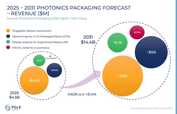
As of 2025, photonics packaging has been driven overwhelmingly by optical transceivers for datacom and telecom. Looking ahead, demand from AI infrastructure, particularly the need for more efficient, higher-bandwidth, lower-power interconnects, will accelerate adoption of CPO in both scale-out and scale-up architectures. Importantly, this shift should not be viewed as a replacement for pluggable optics. The pluggable optical transceiver market is still expected to grow between 2025 and 2031. Rather than displacing them, CPO should be seen as an additional opportunity layer for the photonics packaging ecosystem.
The share of value captured by packaging will, of course, vary by application, depending on technology maturity, manufacturing volume, and the relative importance of assembly complexity. As the optical path moves closer to the logic, first at the EIC level with COUPE-like approaches, and later toward HBM/XPU integration in architectures resembling those pursued by Marvell and Celestial AI, packaging is set to become more demanding and more valuable.
Today, Yole Group estimates that photonics packaging accounts for around 25% of the value in datacom pluggable optical transceivers and about 20% in telecom. In CPO, still in its early phase, photonics packaging could represent roughly 50% of the value at the market’s inflection point in between 2026 and 2027, before declining to around 35% by 2031 as silicon photonics dies capture a greater share of the value chain.
AR represents what could be called the market’s “third application pillar” in the 2031 outlook, and it may prove especially dynamic. Yole Group expects 2026–2027 to mark the inflection point for AR, with 2028 emerging as a key year for microLED as single-panel RGB solutions become ready for mass production. These devices are expected to shrink form factors significantly and support wider adoption.
Eric Mounier, PhD is Chief Analyst, Photonics at Yole Group.
With more than 30 years’ experience within the semiconductor industry, Eric provides daily in-depth insights into emerging semiconductor technologies such as quantum technologies, the Metaverse, terahertz, photonics, and sensing.
Based on relevant methodological expertise and a significant technological background, Eric works closely with all of Yole Group’s teams to highlight disruptive technologies and analyze business opportunities through technology & market reports and custom consulting projects.
Eric has spoken at numerous international conferences, presenting Yole Group’s vision of emerging semiconductor technologies, markets, and applications.
Previously, Eric held R&D and Marketing positions at CEA-Leti (France). Eric Mounier has a PhD in Semiconductor Engineering and a degree in Optoelectronics from the National Polytechnic Institute of Grenoble (France).
Raphaël Mermet-Lyaudoz, PhD, is a Technology & Market Analyst in Photonics and Display, with core expertise in Augmented Reality.
At Yole Group, Raphaël covers diverse photonic/display topics, including AR/VR, MicroLED, photonics packaging, and other innovative topics linked to these themes. He investigates the evolution of these technologies and market trends to deliver in-depth analyses in Yole Group’s products.
Raphaël obtained an Engineering degree from the Institut d’Optique (FR) and a PhD from the Université de Lyon (FR) in collaboration with INL-CNRS. During his academic studies, he focused specifically on Optics, Material Appearance, Nanophotonics, Emerging Materials, and lasers. Raphaël has published various works in peer-reviewed scientific journals.
Source: www.yolegroup.com