Physical design engineer is a specialized function within chip design that encompasses the intricate process of transforming the abstract hardware logic initially delineated in a high-level Hardware Description Language (HDL) into a tangible configuration of physical logic gates and interconnecting wires. This tangible representation serves as the blueprint for the actual fabrication of functional silicon chips.
Physical design engineers play a pivotal role in the chip design process, utilizing sophisticated physical implementation tools to meticulously oversee every phase of the design. Their primary objective is to fine-tune the design across a multitude of critical parameters, including timing, power efficiency, chip area, and adherence to Design Rule Checks (DRCs). Their unwavering focus is on ensuring that the final silicon product not only meets but surpasses all design specifications, resulting in a high-yield, fully functional chip.
Physical Design Engineer – Key Skills and Qualifications
A typical physical design engineer typically holds a degree in Electrical Engineering or Electronics Engineering, often specializing in various levels of expertise. While a Bachelor’s degree may suffice for entry-level positions, advanced degrees (Master’s or Ph.D.) can significantly benefit those aiming for senior roles or specialized positions.
Technical proficiency is a cornerstone for physical design engineers, encompassing a range of skills:
- Mastery in resolving electrical circuits involving diverse components like resistors, capacitors, inductors, and transistors.
- A comprehensive grasp of digital logic gates, encompassing both combinational and sequential aspects, along with their respective transistor implementations.
- Fundamental knowledge of Static Timing Analysis, covering parameters such as setup time, hold time, recovery, and removal.
- Profound understanding of power dissipation sources within a design, including leakage, switching, and internal power, coupled with various optimization techniques like clock gating, power gating, and dynamic voltage and frequency scaling (DVFS).
- Proficiency in using Electronic Design Automation (EDA) tools for synthesis, place, and route processes. A deep understanding of these tools and their underlying algorithms enables informed decision-making.
- Proficiency in scripting and programming languages (such as Tcl, Python, or Perl) is essential. These skills aid in efficiently handling vast amounts of generated data, enabling concise summaries and pinpointing root causes, thereby saving time and effort.
Soft skills also play a vital role in a physical design engineer’s success:
- Problem-solving skills are crucial for addressing intricate design challenges, demanding strong analytical thinking.
- Attention to detail is essential to meticulously analyse designs and avoid common errors.
- Effective communication skills are vital for articulating ideas, collaborating within cross-functional teams, and justifying design decisions.
The Physical Design Engineer’s Workflow
The physical design workflow involves various stages in creating integrated circuits (ICs). The figure describes a typical physical design flow.
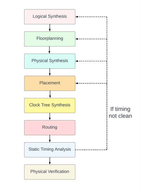
Figure 1: Physical Design Flow
Here’s a detailed breakdown:
- Synthesis: A physical design engineer receives the Register Transfer Level (RTL) description and initiates the synthesis process, transforming it into a logical netlist. During this phase, the engineer synthesizes logical memories into SRAMs and other logic using registers and combinational logic. Additionally, they provide valuable early feedback to RTL designers by identifying paths with significant logic depth, enabling collaborative optimization.
- Floorplanning: Simultaneously, engineers initiate the creation of a floorplan, which encompasses the following key aspects:
- Determining the configuration of the design in relation to other designs and the top-level design structure.
- Specifying the dimensions of the floorplan, taking into account the sizes of macros, standard cells, and the intended utilization targets.
- Strategically arranging the block’s pins while considering the essential data exchange both within and outside the design boundary.
- Floorplan step also draws the power distribution network, places the power switches and other physical-only cells like the endcap cells, well tap cells etc.
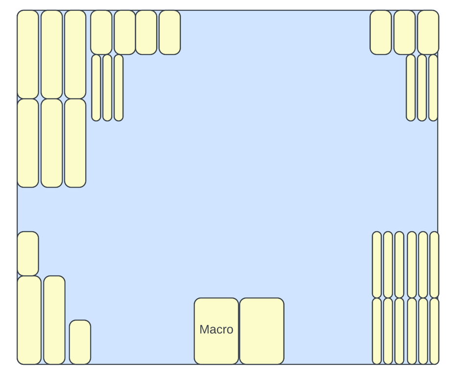
Figure 2: Floorplanning
Once the floorplan is ready, designers can now attempt to run physical synthesis where in addition to the cell delay, they can also get some reasonable net delays along with high fanout synthesis to allow better timing feedback to the RTL designers. It should be noted that during physical synthesis step the signal wires are not actually routed but the routing is estimated with the help of Global Routing (or sometimes Virtual Routing).
- Placement: Placement stage legalizes the standard cells along standard cell rows and refines the cell placement. During placement, designers can also attempt to mitigate placement congestion, convert single bit flip-flops to multi bit flip-flops, perform power optimizations, scan chain reordering etc while considering timing.
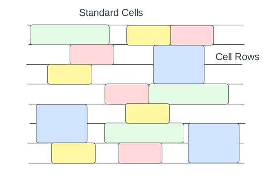
Figure 3: Cell Placement
- Clock Tree Synthesis (CTS): Clock Tree Synthesis step builds the clock network and subsequently routes the clock nets. It optimizes the clock tree network for three main parameters: clock latency, clock skew and the clock transition.
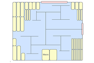
Figure 4: Clock Tree Synthesis
- Routing: During routing, the signal nets are routed on routing tracks while keeping into account the timing, routing congestion, signal crosstalk and other routing DRCs like shorts.
- Static Timing Analysis: Static Timing Analysis is the timing verification step performed at intermediate stage during physical implementation to gauge the timing health of the design. While implementation tool generates their own parasitic data internally to optimize and report timing, the timing tool being a signoff tool relies on more accurate extraction engines to perform the parasitic extraction. STA is typically run on multi-mode and multi-corner method to identify timing bottlenecks like simultaneous setup-hold critical paths early in the design cycle.
- Physical Verification: This steps checks the layout for compliance with design rules to ensure manufacturability and reliability. This includes design Rule Check (DRC) and Layout vs. Schematic (LVS) checks.
Tools and Software
Physical Design Engineers employ a suite of Electronic Design Automation (EDA) tools to meticulously craft, validate, and enhance the physical layout and electrical functionality of semiconductor devices and integrated circuits. This toolkit typically includes:
- Synthesis: Synopsys Design Compiler and Cadence Genus.
- Place and Route: Synopsys Fusion Compiler and Cadence Innovus.
- Static Timing Analysis: Synopsys Primetime and Cadence Tempus.
- Parasitic Extraction: Synopsys StarRC.
- Physical Verification: Synopsys IC Validator and Mentor Graphics Calibre.
- Logical Equivalence Checking: Synopsys Formality and Cadence Conformal.
- EM/IR Analysis: Ansys Redhawk and Cadence Voltus.
- Low Power Verification: Synopsys VCLP.
- Power Analysis: Synopsys PTPX and Ansys Power Artist.
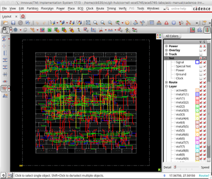
Figure 5: Cadence Innovus GUI for physical implementation
These tools collectively empower engineers to fine-tune, validate, and optimize semiconductor designs, ensuring optimal performance, adherence to design specifications, and robust functionality.
Challenges in Physical Design Engineering
Physical Design engineers encounter an array of challenges throughout their work:
- EDA Tool Reliability: Physical design engineers heavily depend on EDA tools for implementation and convergence. However, instances occur where these tools do not function as advertised. This necessitates seeking recommendations and guidance from application engineers to explore alternative approaches or strategies to meet the objectives.
- Lengthy Run Times: The duration of runs depends on factors like block complexity, size, and the number of cores utilized. Longer run times limit the number of design iterations, impacting the ability to converge on an optimal design. Increasing core usage to expedite runs may restrict the ability to concurrently conduct multiple experiments for convergence.
- Corner Case Challenges: Physical design engineers frequently encounter unexpected corner cases within their designs, necessitating custom solutions to mitigate the impact on Quality of Results (QoR). Each design phase may unveil unique corner cases demanding innovative design approaches.
- Navigating Trade-offs: Balancing power, performance, and area presents an ongoing dilemma. Physical design engineers continually navigate trade-offs, understanding that achieving the best in all aspects simultaneously is unfeasible. Much of the effort in physical design engineering revolves around pinpointing the ideal balance aligning with design targets.
Trends and Innovations
Here are three notable trends and innovations in physical design engineering:
- Advanced Process Nodes and Design Challenges: As semiconductor technology continues to push towards smaller nodes (such as 5nm, 3nm, and beyond), physical design engineers face unprecedented challenges. Shrinking transistor sizes amplify issues like increased leakage, variability, and complex parasitics. Innovations in design techniques, like EUV lithography and new materials, are emerging to tackle these challenges. Additionally, novel methodologies for layout optimization and timing closure become crucial to ensure chip performance and functionality.
- AI and Machine Learning in Physical Design: AI and machine learning are making significant inroads into physical design engineering. Engineers are leveraging AI algorithms for tasks like floor planning, placement, routing optimizations, and timing closure. These technologies offer the potential to automate and expedite repetitive tasks, optimize designs for performance and power, and explore design spaces more efficiently, leading to faster time-to-market and improved quality of results.
- Heterogeneous Integration and System Design: There’s a growing trend towards heterogeneous integration, combining diverse technologies like CPUs, GPUs, memory, and specialized accelerators into a single chip or package. This shift demands innovative physical design approaches to harmonize different components with varying characteristics and optimize interconnects for efficient communication. 3D integration, chiplets, and advanced packaging techniques are becoming more prevalent, demanding novel design strategies to ensure seamless integration and optimal performance.
These trends underscore the ongoing need for inventive solutions in physical design engineering to overcome the challenges posed by cutting-edge technologies and to enable the development of more powerful and efficient semiconductor devices.
Career Opportunities and Job Outlook
The job market for physical design engineers has been historically robust due to the increasing demand for semiconductor products across various industries like technology, automotive, healthcare, and more. Physical design engineers play a crucial role in the semiconductor industry, as they are responsible for designing and implementing the layout of integrated circuits (ICs) on silicon chips.
Career opportunities for physical design engineers can be promising, with roles available in:
- Semiconductor Companies: Major semiconductor companies such as Intel, AMD, NVIDIA, Qualcomm, and TSMC are always seeking skilled physical design engineers to work on cutting-edge chip designs.
- Electronic Design Automation (EDA) Companies: EDA companies like Cadence Design Systems, Synopsys, and Mentor (now part of Siemens) develop software tools used in the design and verification of ICs. They hire engineers to work on tool development, optimization, and support.
- Startups and Small Firms: Emerging companies focusing on specialized chips, AI hardware, IoT devices, RISC-V and niche technologies often look for physical design engineers to create innovative chip designs.
- Research and Development: Opportunities exist in research institutions and academia for those interested in pushing the boundaries of chip design through innovative research.
- Consulting and Services: Some engineers choose to work as consultants, providing expertise to multiple companies or offering specialized services in chip design.
The career path for physical design engineers often begins with entry-level positions such as Physical Design Engineer or CAD Engineer, gradually progressing to roles like Senior Physical Design Engineer, Lead Engineer, and eventually, managerial positions.
Continuous learning and staying updated with the latest advancements in semiconductor technology, tools, and methodologies are essential for career growth in this field. Specializations in areas like advanced process nodes, low-power design, or specific applications (such as AI chips or IoT devices) can also enhance career prospects.
In chip design, physical design engineers make ideas real by turning them into silicon chips. They are like expert builders, carefully handling every step to create high-quality chips that work well. They focus on making sure everything- like timing and power- works perfectly. This job involves using special tools and skills to make sure the chips meet all the requirements and work even better than expected. It’s a field that’s always changing and offers a chance for people to be creative while making technology better.


