In this post, we will highlight some tips for a physical design engineer that they might find useful in their job:
1. A Script in Time Saves Nine
Just like any job, physical design can be repetitive. Scripting serves two purposes:
- Automating repetitive tasks: Any repetitive task can potentially become monotonous and mundane in no time. Scripting those tasks helps you get the job done quickly while leaving you time to focus on more important tasks.
- Data Mining: Modern designs are huge and there is a plethora of input variables that can change and a gamut of output parameters that one need to evaluate to decide on a working recipe. Scripting can glean useful information out of one or more text files comprising a few million lines each and create a concise summary of what transpired in each run and what are the next action items.
There could be multiple scripting languages of choice.
- Most of the backend physical design tools have a Tcl interface and it is very helpful to write a Tcl script to get the information out of the EDA tools.
- Off late, there are a few tools that have a Python interface and python is a very strong language for gleaning out information out of text files, or perhaps draw histograms, generate statistical data or even help visualize the results better.
- Most of the tools have UNIX terminals and Shell scripting can help automate the process of dispatching jobs.
2. Befriend Log Files and Reports
Log files are a physical design engineer’s best friend. Log files, depending on the extent of its verbosity, contain useful messages that fall under three major categories:
- Information – Information messages typically inform the user of the operation that is currently being performed under the hood.
- Warning – Warnings are non-fatal messages that may warn the user of missing input(s) or some assumptions that the algorithm made to make forward progress and would like to user the review or correct the inputs for the next run.
- Error – Error messages are usually fatal (sometimes non-fatal too) that the tool or the algorithm is not able to resolve, and it is requesting the user to take immediate action in order to make progress. Non-fatal error messages also imply that the results cannot be trusted and therefore may pose a risk for sign-off.
Reports are more detailed summaries of a particular task that was performed by the EDA tool. Like it may summarize the timing QoR, or provide a detailed area breakdown or power numbers divided into individual components etc. These are useful to gauge the quality of results and may also guide the designers on what the next steps should be.
3. Physical Design is all about Making the Right Trade-offs
Nothing comes for free when it comes to physical design. Everything is a trade-off. The key metrics that any physical design engineer cares about are- performance, power, area, routability, voltage drop, physical DRCs, verification complexity etc. Let’s look at some trade-offs:
- Pushing the design performance means being able to operate at a higher clock frequency to increase the system throughput. This comes at the cost of increased design area owing to the usage of bigger and faster cells, which in turn also increases the power consumption of the design owing to the usage of power-hungry leakier cells.
- Achieving high design utilization directly translates into smaller floorplan area, however, this comes at the cost of fewer routing resources available and an increase in the design DRCs. Also, increased cell density may also result in dynamic voltage drop hotspots that can potentially limit the max frequency of the design or increase the overall power dissipation.
- Decreasing the power dissipation of the design by using power gating or voltage islands comes at the cost of increased complexity during design verification where we need to ensure switch chaining is correct for power switches, and all the voltage crossings have an isolation cell or a level shifter to ensure correct operation of the design.
These are some of the trade-offs that physical design engineers need to make on a day-to-day basis. Choosing the right trade-offs for your design is critical where one must strive to strike the perfect balance between performance, power, area consistent with their design specifications. This is one reason why physical design engineers should go through the entire flow, including sign-off to determine impact of any recipe changes on all sign-off domains like timing, physical verification, EM/IR, power etc.
4. Garbage-in Garbage-out
There are several collaterals needed as inputs to the physical design space. These may include RTL, the design constraints in the form of SDC, the low power specification in the form of UPF, the technology collaterals like the instance LEFs, LIBs etc. Always double check the quality of the inputs because physical design is a machine where if you put in garbage, you will only get garbage at the output. As an example:
- RTL: The RTL could be fundamentally broken if the sub-modules within the top-level scope are not hooked-up. Using such an RTL, one might be able to synthesize the individual sub-modules, but the missing connections would mean that the relative placement of the sub-modules and the routing congestion numbers of the top-level implementation run cannot be trusted.
- UPF: Unified Power Format defines the low power specification of the design that includes the power domain definitions, the power state table, the isolation and level shifter strategies, power switch strategies etc. Incorrect UPF would mean incorrect implementation of the low power specification.
- SDC: Standard Design Constraints defines the timing constraints like clock definition and clock frequency, input transition, output load, clock groups and other timing specifications. Incorrect SDC can directly lead to aggressive or sub-optimal optimization.
5. Catch 22- Simultaneous Setup-Hold Critical Paths
Quite often physical design engineers find themselves in a catch 22 situation where the same timing path is setup critical in one corner and hold critical in another corner. There are quite a few possible solutions to get out of this situation.
- Crosstalk noise: Any crosstalk noise rising due to capacitive coupling between the victim nets of the timing path with aggressor nets in the vicinity impacts both setup and hold timing. Fixing the crosstalk noise on these victim nets will help improve both the setup and as well as the hold slack on the timing path, thereby offering more leeway to the designers to attempt traditional timing fixes to close setup or hold.
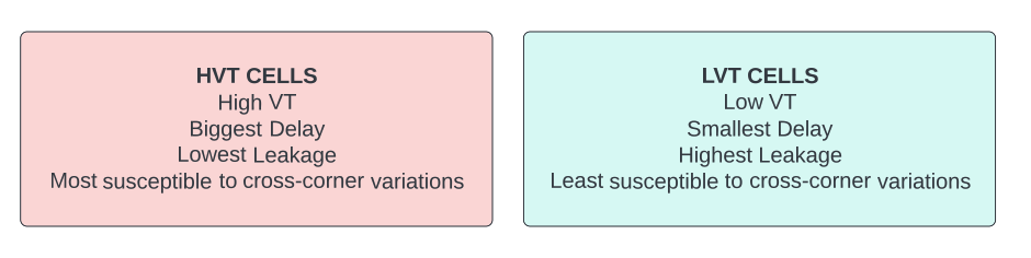
- Reduce the usage of high Vt cells on the critical path: The high Vt cells (HVT) cells exhibit quite large delay variation across corners and converting these HVT cells to a lower Vt flavor (SVT or LVT) typically helps alleviate setup-hold criticality. Downside is slight increase to the leakage power, but again that’s the right trade-off to make.
6. Clock is the Lifeline of your Design
The clock signal is the fastest signal and flows throughout the design just like blood does in a human body. Clock implementation is therefore quite important and demands extra attention and care.
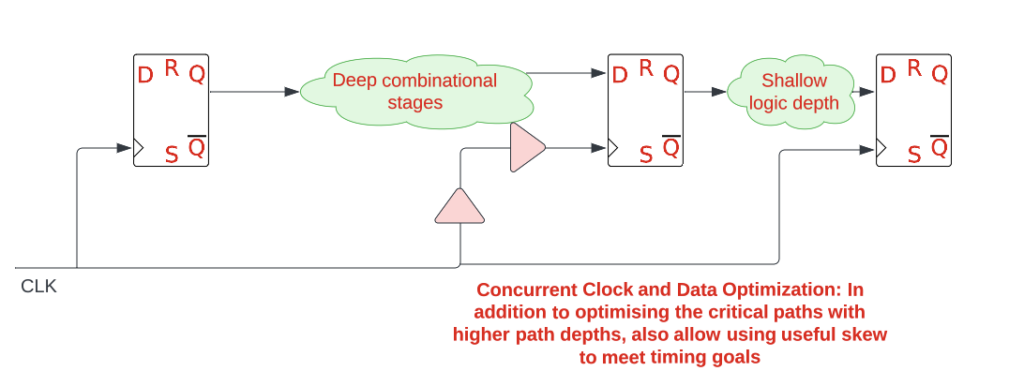
- Concurrent Clock and Data Optimization (CCD)- Concurrent Clock and Data Optimization is an optimization technique that optimizes the data path in conjunction with the clock path. This may involve skewing the clock to a few registers to gain useful skew to meet timing on critical paths. While this is a great technique, but it might result in insertion of many more hold buffers in the design. It might be prudent to limit the max prepone or postpones while employing CCD.
- Clock Transition- Clock trees are designed to have sharper clock transition because slower clock transitions results in higher crowbar current, and hence higher short circuit power in the design. However, in order to maintain a sharper transition, designers might limit the maximum route length of their clock nets, thereby inserting more repeaters and burning more dynamic power.
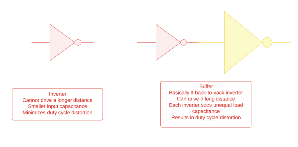
- Inverter versus Buffer Clock Tree- Designers are often confronted with the decision of making a choice between using inverters or buffers for building the clock tree. More often, inverters are chosen because they help lower the duty cycle distortion. However, using buffers have their merits in the sense that a buffer can drive a longer distance in contrast to an inverter of the same drive strength.
- Clock NDRs (Non-Default Rules)-
Shielding: Clock routes are often shielded with power or ground nets to minimize the coupling to/from the signal nets in the vicinity. These routes can be shielded on both sides (full shielding) or only on one side (half shielding). Full shielding adds load capacitance and therefore slows down the clock signal, and it could result in slower clock transitions.
Non-default width: In addition to shielding, clock routes are usually routed in the non-default width as thicker wires to minimize the delay.
Spacing: If not shielding, sometimes the tracks adjacent to the clock routes are left vacant, again to minimize the coupling to/from the signal nets in the vicinity.
- Clock VT choice- Always limit the clock repeaters to a single VT type and not allow mixing of VTs. This is because cells of different VT flavors have different scaling across corners and therefore may result in lower silicon yield.
7. With Great Power Comes Great Responsibility
Power consumption is a growing concern for modern SoCs and engineers face an uphill task to find innovative solutions to increase the time needed for the next recharge. This is particularly true for mobile devices. Architects and physical design engineers have many low power techniques at their disposal to achieve this:
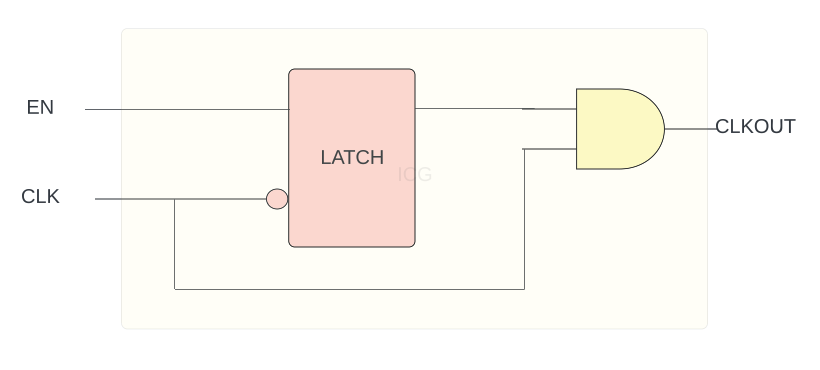
- Clock Gating: Gating the clock when the registers are not expected to change their output states can result in saving the dynamic power dissipation of the design. This is accomplished by using clock gating cells in the design.
- Power Gating: Turning off the voltage supply to a circuitry or a sub-block when not functional can not only save the dynamic power but also significantly cut down on the leakage power. This is accomplished by using power switches, though it comes with the extra baggage of managing the voltage islands, insertion of isolation cells and level shifters and other constraints like managing the in-rush current.
- Register Banking: There are quite a few buses present in any design with similar but distinct logic. Instead of using a traditional one-bit register, modern libraries have banks of registers that may be 2-bits, 4-bits or even 8-bits in a single standard cell. This results in higher packing density, but more importantly fewer clock pins to route the clock to, thereby resulting in lower clock power dissipation.
- Usage of high-VT cells: High VT cells (HVT) cells, though slower, have orders of magnitude lower leakage in contrast to their low VT (LVT) counterparts. Using HVT cells on non-critical timing paths can lower the standby leakage power of the design.
8. Always Expect the Unexpected and Leave Room for Late Surprises
Physical Design lies in the last mile stretch to tape-out and is prone to surprises. Physical design engineers should always keep room for unexpected surprises that may come up a few days before the tape-out. As an example:
- RTL Bug: There may be a functional RTL bug discovered a few days before tape-out, and physical design is expected to take in the ECO (Engineering Change Order) that may be anywhere between few tens to few hundreds of gates, may or may not be timing critical and may or may not need to go into a physically congested region.
- Hold Timing Closure: Hold Timing closure entails adding buffers on the hold critical nodes and adds up to the placement congestion of the design. Physical design engineers must leave some physical placement blockages particularly around the hard macros to leave room to add hold buffers at the very end of the tape-out cycle.
- EMIR Fixes: Some EM/IR feedback always come late in the cycle, particularly the ones that are a result of a functional vector. These fixes can potentially disrupt timing and physical design engineers may run into chicken and egg problem. This is where leaving some guard band in the form of uncertainty might help.
9. Being in Touch with Fundamentals
Once in the industry, we all tend to take the fundamentals for granted. However, being in touch with the basics will be immensely helpful in understanding the trade-offs involved and make better engineering calls. MOS transistor theory, fundamentals of digital logic design, fabrication process, fundamentals of setup and hold timing, operation of a 6T SRAM cell are some fundamentals that are taught in school and though physical design engineers may not make use of these fundamentals (except perhaps the setup and hold timing) during their day-to-day work, will be immensely useful.
10. Stay Curious, Stay Inquisitive
It is hard to overstate the significance of reading technical literature in the form of white papers, IEEE papers, technical presentations and even blogs to gain insights into various scenarios that you may not have encountered in your designs yet, but will give you an idea of the available solution space to motivate a better implementation. Similarly, asking questions and discussing alternate implementations without the fear of being judged will help you grow into a better physical design engineer.


