

Power gating is a technique used to reduce ASIC and SoC power consumption by turning off parts of the design that are not being used or in inactive mode. Also, it is a very efficient technique to reduce leakage power in ASIC designs.
The basic concept is to have essentially two power modes:
At any time during the operation, the design should switch between these two modes in such a manner as to increase power savings while having minimum impact on performance.
The supply power to the inactive blocks can be turned off using:
While power gating is the primary technique for leakage power reduction for idle parts of the design, it can be combined with state retention and standby voltage scaling techniques for improving energy and ramp-up latency.
Most of the CMOS logic circuits are usually a combination of p-channel transistors (pull-up network) and n-channel transistors (pull-down network). The CMOS circuit keeps on dissipating power in the absence of any switching activity due to the leakage current flowing from VDD to the ground (as shown in Fig. 1.1).
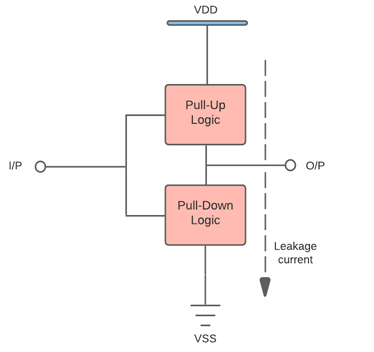
Fig. 1.1: Leakage in basic CMOS circuit
One simple solution in such a situation is to disconnect the path to the power and ground terminals. This can be done by adding a power gating circuit that can disconnect the path when the circuit is in inactive mode.
A simple example of a CMOS circuit with power gating is shown in Fig. 1.2. Here the sleep transistors also called switch cells, are controlled by a SLEEP signal which is used for active or inactive mode of operation.
When SLEEP = OFF(0),
When SLEEP = ON(1)
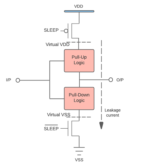
Fig. 1.2: Power gating in CMOS
Adding the switch cells split the power supply of the design into a permanent power network that is connected to the global power supply and a virtual power network that drives the gated logic and can be turned off in inactive mode.
Note that the switch cells also contribute to extra leakage power when they are on as because they are made of active transistors. But the leakage power from them is usually quite small as compared to the gated logic.
The sleep transistors also called switch cells, can be divided into two categories :
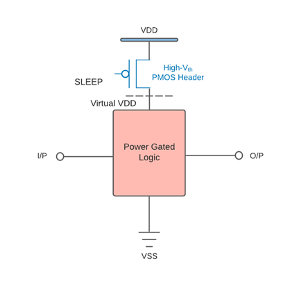
Fig. 1.3: Header Switch Cell
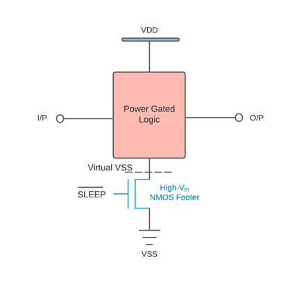
Fig. 1.4: Footer Switch cell
These switch cells design require very careful sizing. During the active mode, they should add minimal delay to the circuit and they should have low leakage during sleep mode.
In real designs, a single switch cell is not in any way sufficient to provide power to the whole logic. So a network of switch cells is used to achieve low voltage ramp-up time and avoid IR-drop related issues.
In a design, any one of the Header cells or Footer cells can be used for power gating. Alternatively, a combination of Header and Footer cells can also be implemented for the same.
The control to the switch cell network is generated by the power gating control block in the design.
There are two ways in which power gating can be implemented in an ASIC design:
In Fine-grain power gating, a switch transistor is integrated inside the standard cell logic. The switch transistors are designed by either a library IP vendor or a standard cell designer. The virtual power or ground supply rails are also added inside the standard cells.
Fine-grain power gating has the advantage of being easy to implement. Usually, these integrated standard cells follow the normal standard cell rules and can easily be handled by EDA tools for physical design implementation. In addition to that, fine-grained power gating is very flexible for controlling the supply. Power can be easily shut off to idle individual blocks or even to individual cells without shutting off the power to other cells or blocks which continue to operate. This can result in very efficient leakage power reduction.
The size of the gate control logic is usually designed for the worst-case scenario that this circuit can switch through each clock cycle which increases the size of the switch transistor. Thus, adding a switch transistor to each cell leads to increased area penalty. Also, individually gating the power of every cluster of cells can also create timing issues because of the voltage variation between the cluster which can be difficult to resolve.
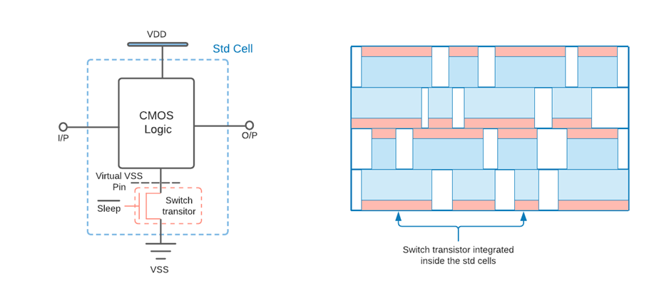
Fig. 1.5: Fine-grain Power gating
In coarse-grained power gating, as the name suggests power is gated very coarsely in the design. This approach uses a distribution of switch cells in the design which control the power-gating of logic locally through a shared virtual power network. In this type of power gating, the switch cells are a part of the power-grid network rather than the standard cell itself.
There are two types of coarse-grain structure that can be implemented:
Ring-based: The switch cells are placed as a ring around the perimeter of the logic block that needs to be turned on and off during the operation. This simplifies the power-grid structure inside the block.
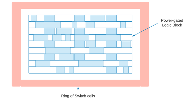
Fig. 1.6: Ring-based Coarse-grain Power gating
Column-based: The switch cells are added as multiple columns within the logic block. Here the global power grid inside the block is routed in the higher metal layers, while the switched power rails are routed in lower layers.
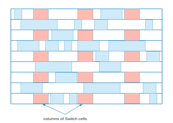
Fig. 1.7: Column-based Coarse-grain Power gating
Coarse-grain power gating has the advantage of less area overhead as compared to fine-grain power gating. This approach is also comparatively less sensitive to PVT variation and results in less IR-drop variation.
However, this approach results in lesser leakage power reduction as compared to fine-grain power gating. Also, in coarse-grain power gating, simultaneous switching capacitance is a major concern. In order to limit simultaneous switching of all the cells, the switch cells can be connected in a daisy chain fashion or blocks of switches can be turned on selectively by using special counters.
Isolation cells are used to isolate the power gated logic domain from the always-on logic domain. These cells essentially act as a buffer with a control signal. When the control signal is enabled the cell acts as a buffer and when it is disabled the cell provides a constant logic 0 or 1 at the output.
Whenever a logic is power-gated, the output signals from the gated block needs to be controlled. As soon as the power is gated, the output signal will start to float to unknown values. Now consider a scenario where these signals might be driving some cells in the always-on domain. Such cells will give incorrect output if they receive unknown or floating values as inputs. These signals can be isolated by assigning either logic 0 or logic 1. Normally, these static values (reset value or off state value) are sufficient to continue the normal functioning of the always-on domain cells. This is where Isolation cells are used.
Isolation control signals are controlled by a power gating controller. Usually, a simple OR or AND logic can serve the purpose of output isolation. An example of an isolation cell using an AND gate is shown in Fig. 1.7.
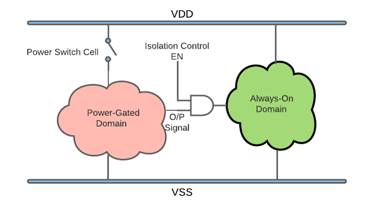
Fig. 1.8: Signal Isolation using AND gate
Here, if
Isolation cells have additional complexity in that they have two power domains, the power-gated domain, and the always-on domain. To enable the power supply tapping from the pg-grid in both domains, these cells are placed closer to the boundary of the two physical domains.
Whenever a design is power gated, the design needs some kind of state retention, so that the internal states of the power gated logic can be preserved during shut-off mode and loaded back to it when the logic is reactivated. A simple technique is to load the data into memory before shutting down the block and when the block is powered up, the values are scanned back from the memory. Without state retention, the design will have to be reconfigured each time it is powered up.
Retention registers are special low-leakage flip-flops that are used to hold the data of a power gated logic block. These registers can retain critical data during the power-off and transfer it back to the logic block when power is turned back on. Retention registers are supplied with a continuous power supply. A power gating controller is used to control the retention mechanism such as when the power gated block data needs to be saved and when to restore it back.
The retention strategy is highly design-dependent. For example, the FSM states in the design or data of some critical configuration data can be retained which decides the mode of operation in the design.
The addition of retention registers in the design adds overhead in terms of area and implementation complexity. Due to the area and routing overheads, they are used in very specific cases, where fast wake-up of the gated domain is required, and reconfiguring the gated domain each time is not desirable.
For reducing the ramp-up times, saving and restoring the states quickly and in a power-efficient manner is very critical to get the block fully functional after power-up.
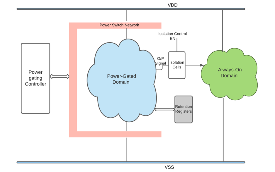
Fig. 1.9: block design with power gating
Although power gating is a very powerful technique to reduce leakage power, but it comes with its own set of challenges.
DFT for power-gated designs has its own set of new challenges. For example, the various power domains need to be controlled and stabilized during the test mode, and how to add controllability and observability for the low-power design elements such as switch cells, isolation cells, state retention registers, etc., and how to minimize the power during the testing process.


