

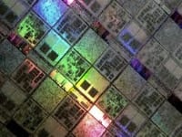
Semiconductor wafer is absolutely invisible in our daily life but it exists in a form of an ASIC or an IC in each and every electronic device we use. Semiconductor wafer is a round piece of silicon which consists of silicon dies that are designed to perform a very specific functionally. One can easily remember from school that silicon has an atomic number of 14 on the periodic table and has an atomic weight of slightly more than 28. But there are many other interesting facts you should know about semiconductor wafer.
Here are 10 important facts you need to know about semiconductor wafers:
1. Semiconductor wafers are made of silicon which is the second-most common element on the Earth (just after oxygen) and it’s the seventh-most common element in the entire universe.
2. As the sand used to produce the semiconductor wafers has to be a very clean, most of the sand used for these processes is shipped from the beaches of Australia. Not just any sand scraped off the beach can be used for semiconductor wafer production.
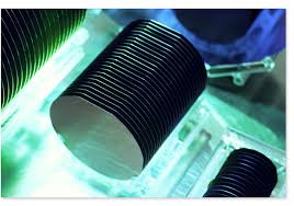
3. Semiconductor wafers are available in a variety of diameters. In 1960 the first semiconductor wafer was manufactured in the US, the semiconductor wafer’s diameters was 1 inch. Today the standard semiconductor wafer size is 12 inch with foreseeable plan to achieve 18 inch semiconductor wafers.
4. Wafers are formed with a highly pure, almost defect-free single crystal material. The process to forming these conductors is called Czochralski. During this process, silicon or germanium is made by pulling a seed crystal from a melt. Baron or phosphorus can be added to the molten intrinsic material in direct amounts in order to dope the crystal. After doping the crystal the material is then turned in to a n-type and p-type extrinsic semiconductor.
5. Semiconductor wafers thickness will vary greatly. Wafer thickness is always determined by the mechanical strength of whatever material is used to make it. No matter what the semiconductor is made out of, the wafer has to be thick enough to support its own weight so it doesn’t crack during the handling process.
6. The use of extrinsic (pure) semiconductor wafer can be seen in many everyday electrical devices. An extrinsic semiconductor is a semiconductor that has been doped and is transformed in to a pure semiconductor. Applications such as Laser, Solar Cells are based on extrinsic semiconductor.
7. Even though silicon is considered to be the most prevalent material for wafers that are used in electronics, other compounds can be used as well. III-V or II-VI materials have also been used. Gallium arsenide or (GaAs) is a IIIV semiconductor that is produced during the Czochralski process. It’s often used as a common wafer material.
8. Die per wafer calculation is the first step for every engineer that wishes to find out the price of each die on a semiconductor wafer. Gross number of dies per wafer can easily and quickly calculated using AnySilicon free tool here.
9. In some specific applications the die per wafer is equal to 1 (one) which means that there is a single die on each semiconductor wafer. As the maskset reticle cannot cover the entire semiconductor wafer, a special stitching needs to be performed to connect the different tiles together. Some silicon wafer suppliers have very good experience in these types of applications.
10. Proper storage conditions are necessary to prevent contamination and/or degradation after shipment. Semiconductor Wafers that are not vacuum sealed must be placed in a Nitrogen (N2) cabinet with a flow rate of 2 to 6 SCFH (Standard Cubic Feet per Hour).
