Deep Trench Isolation (DTI) works by creating deep, narrow trenches in silicon substrates that effectively isolate active regions of a chip. This technique not only enhances device performance but also prevents interference between components, ensuring integrity in complex circuits. The innovative design of DTI structures plays a crucial role in the advancement of various semiconductor applications.

Figure 1: Deep Trench Isolation (credit: Bomy Chen)
Deep trench isolation (DTI) is vital in semiconductor technologies. It creates barriers within electronic devices to improve performance. Here’s why DTI is important:
Key Components of DTI:
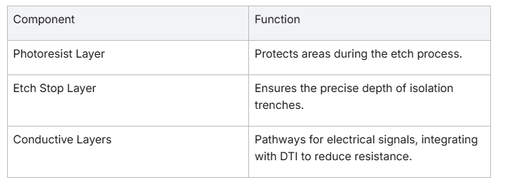
DTI begins with the application of a photoresist layer. This is followed by creating trenches using an etch process. An Etch Stop Layer defines the trench depth. Finally, dielectric materials fill the trenches to form deep trench isolation regions.
In the realm of semiconductor technologies, DTI is a key technique. It facilitates the high performance and reliability of modern electronic devices. Understanding DTI’s process flow and utility is indispensable for advancing device architectures and efficiently managing conductive layers.
Deep trench isolation (DTI) is a process used in semiconductor fabrication. It creates trenches, or barriers, within electronic devices to separate components. This improves their performance by enhancing the flow of electrical signals and reducing interference.
DTI structures enable the integration of numerous components on a single chip. They allow for high-density integration, which leads to more compact and efficient devices.
The formation of deep trench isolation structures starts with the application of a photoresist layer. This layer protects certain regions of the chip during an etch process. Next, trenches are made into the silicon using this process. An Etch Stop Layer is crucial here. It ensures that the trenches have the correct depth for effective isolation.
After the trenches are formed, they are filled with dielectric materials to create the deep trench isolation regions. These materials act as insulating barriers, preventing unwanted interactions between the conductive layers in the device.
DTI adds mechanical strength to electronic devices. By using materials like Polycrystalline silicon and high-reflectivity metal layers, these structures resist cracking. This not only extends the life of the device but also enhances its reliability.
Maintaining device integrity is crucial. DTI’s precise trench creation and filling processes help avoid structural failures. The method ensures that semiconductor devices remain efficient and robust against everyday stresses.
Deep trench isolation (DTI) is essential in modern electronic devices. It separates different components on a chip. This reduces electrical interference. DTI is useful in many applications, which we will explore below.
In high voltage applications, DTI plays a crucial role. It allows devices to handle high electric power without failure. The deep trench isolation structures provide strong separation. This helps manage heat and avoid shorts between conductive layers.
DTI significantly impacts Silicon On Insulator (SOI) devices. These devices have a thin silicon top layer. This layer is above an insulating substrate. Deep trench isolation regions improve device performance. They decrease parasitic capacitance and enhance the signal quality. This makes SOI devices more efficient and reliable.
Smart power processes benefit greatly from DTI. The technology helps in managing power more efficiently. It uses deep trench processes and enables precise control over electrical signals. This results in enhanced device performance and reduced energy loss. Here’s a brief overview of how DTI aids in smart power processes:
DTI influences various aspects of technology. Its applications range from high voltage systems to smart devices. As semiconductor technology advances, DTI will continue to be essential in creating better electronic solutions.
Deep trench isolation (DTI) is a crucial technology in the fabrication of modern electronic devices. It involves creating deep trenches in a semiconductor substrate, which are then filled with dielectric materials to isolate different regions of a chip. By effectively reducing parasitic capacitance, DTI enhances device performance and reliability.
Deep trench isolation structures play a vital role in boosting device performance. They help in the precise isolation of electronic components, minimizing interference between them. With reduced parasitic capacitance, electrical signals can travel more efficiently across conductive layers. This leads to faster processing speeds. Shallow trench isolation (STI) might offer some of these benefits, but DTI goes deeper, providing the best results for high-performance applications. Additionally, deep trench structures are compatible with a variety of dielectric materials and conductivity types, allowing for flexible design options.
Reliability is key in electronic devices, and DTI significantly contributes toward this. By employing deep trench isolation regions, devices experience less signal leakage and other electrical issues. This isolation technique serves as a robust Etch Stop Layer, which ensures the integrity of the circuitry. Furthermore, the use of a high-reflectivity layer or high-reflectivity metal layer in the process flow can enhance protection against overheating or damage. With the inclusion of Polycrystalline silicon as a seed layer, DTI ensures that the devices maintain consistent performance over time.
In summary, deep trench isolation not only promotes enhanced performance but also offers improved reliability for electronic devices. The box isolation technique and alternative embodiments make it a versatile choice for future technology applications.
Deep trench isolation (DTI) is crucial for creating isolated regions in electronic devices. However, it comes with several challenges. Managing the etch process is complex, as it requires precise control to form deep trench isolation structures without damaging nearby zones. The selection of materials like dielectric materials and polycrystalline silicon is essential to ensure stability and performance. Additionally, DTI must minimize parasitic capacitance to prevent unwanted electrical signals from affecting device functionality.
Optimizing the process flow in deep trench isolation is vital for efficiency and reliability. One method involves using a photoresist layer to define areas where trenches need forming. The etch stop layer ensures the process halts at specified depths, which avoids over-etching. Alternative embodiments, such as using conductive layers, may enhance conductivity type and electrical isolation. These adjustments aim to reduce production time and improve device performance.
Improving gate oxide yield is a focus of deep trench processes. Etch techniques and dielectric materials must be carefully chosen to protect sensitive layers. A high-reflectivity layer or metal layer is sometimes used to prevent defects. It’s crucial to ensure that the deep trench structures don’t introduce faults in the gate oxide. By refining the seed layer application, manufacturers can achieve a better oxide yield and enhance overall device quality.
These careful optimizations protect against faults and defects, ensuring a successful and reliable deep trench isolation process.
Deep Trench Isolation (DTI) and Shallow Trench Isolation (STI) are both vital in semiconductor manufacturing. Here is a quick comparison of DTI with other isolation techniques like STI and box isolation.
Deep Trench Isolation (DTI):
Shallow Trench Isolation (STI):
Box Isolation:
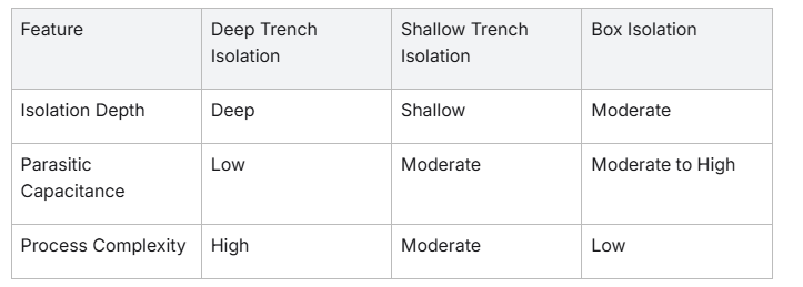
In summary, DTI is suited for applications needing deep isolation and low parasitic capacitance, while STI is better for surface isolation in dense layouts. Box isolation offers a simpler alternative for basic needs.
Deep Trench Isolation (DTI) technology has seen significant progress. These advances help improve electronic devices by enhancing their performance and efficiency. DTI reduces unwanted electrical signals, known as parasitic capacitance, which is crucial in high-frequency applications. Recent innovations focus on optimizing the etch process, improving conductivity types, and utilizing high-reflectivity layers.
Bonded wafers are transforming device fabrication. By stacking different layers like a photoresist layer and an Etch Stop Layer, these wafers optimize the manufacturing process. This technique is used for creating deep trench isolation regions. It enables precise control over conductive layers and ensures high-quality device performance.
Key benefits of bonded wafers:
Innovations in DTI structures focus on the composition and layout of deep trench isolation regions. Using dielectric materials and high-reflectivity metal layers enhances the DTI structure’s efficiency. These innovations aim to create deeper isolation with reduced process complexity.
These advancements in DTI technology enable the development of faster and more efficient electronic devices, paving the way for future innovations.
Deep trench isolation (DTI) technology is crucial in developing efficient electronic devices. As we look to the future, several trends are shaping the field.
Emerging Trends:
These trends indicate a promising future for deep trench isolation, advancing both the design and functionality of electronic devices.
Deep Trench Isolation (DTI) plays a crucial role in modern electronics. It helps in separating individual components on a semiconductor chip. This separation is vital for avoiding electrical interference. DTI improves the performance and reliability of electronic devices.
The DTI Process Flow includes several steps, such as applying a photoresist layer, executing an etch process, and using etch stop layers. These steps create deep trench isolation structures, which are crucial for high-performance electronics.
In conclusion, deep trench processes and structures are vital for producing efficient and reliable electronic devices. They enable designers to use complex layouts without compromising on performance. DTI continues to be an essential component in advancing technology in consumer and industrial electronics.
DTI is a key technology in modern CMOS image sensors. It involves etching deep trenches into the silicon substrate, which are then filled with insulating material. These trenches effectively isolate individual pixels, preventing crosstalk (light or electrical signals spilling over from one pixel to another). This is particularly critical as pixel sizes shrink, allowing for higher resolution sensors without compromising image quality.
DTI offers several benefits:
Deep trenches are typically fabricated using a specialized etching process known as the Bosch process. This involves alternating steps of etching and passivation, gradually creating deep, narrow trenches with high aspect ratios (depth to width).
Initially, introducing DTI can increase dark current and noise due to the exposed sidewalls of the trenches. However, techniques like doping the sidewalls or refilling trenches with biased materials like polysilicon or tungsten can effectively mitigate these issues.
As pixel size decreases, the risk of crosstalk increases. DTI effectively isolates even tiny pixels, allowing manufacturers to continue shrinking pixel dimensions without sacrificing image quality. This is crucial for achieving higher resolution sensors.
DTI allows for the integration of deep trench capacitors within each pixel. These capacitors provide additional storage for electrons when the photodiode saturates, effectively extending the pixel’s full well capacity and enabling a wider dynamic range.
DTI will remain a fundamental technology for future advancements in CMOS image sensors. It will continue to enable smaller pixels, higher resolutions, improved sensitivity, and new functionalities like stacked sensors with multiple layers of silicon for even greater performance enhancements.