A through silicon via, also abbreviated as TSV, is basically a connection that passes through the silicon wafer. These connections are considered to be extremely high performing and high quality interconnects, especially when creating three dimensional integrated circuits and packages. This is because they can be used for vertical stacking to allow the various integrated circuits placed on top of a single 3D package to consume less space yet still have high connectivity and performance. They also allow for interposer layers in between the integrated chips to further increase the size and width of the 3D package in terms of capacity and performance, yet as small and flat as possible when it comes to physical dimensions.
Through-Silicon Via (TSV) technology is a sophisticated method employed in semiconductor manufacturing for creating vertical electrical connections through a silicon wafer or die. Its development, aimed at addressing the limitations of traditional wire bonds and flip chips, heralds a new epoch for 3D integration and circuit density.
The conceptual roots of TSVs span back to the mid-20th century. However, it wasn’t until the 2000s that they began to see practical use, which coincided with the demand for higher performance and smaller form factors in electronic devices.
Significant milestone years in TSV history:
These advancements laid the groundwork for a new approach to circuit board design. Leveraging the vertical integration that TSVs enable, manufacturers have created 3D packages, vastly improving interconnect density and signal integrity while simultaneously reducing footprint size.
Modern TSV processes involve intricate steps such as deep reactive-ion etching for via formation, deposition of a barrier layer to prevent leakage current, and electrochemical deposition to fill the vias with a conductive material, typically copper. The resulting 3D stacked structures are mileposts reflecting the ongoing journey toward unprecedented levels of integration and performance in semiconductor technology.
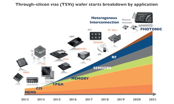
Through-Silicon Vias (TSVs) shows constant growth in the semiconductor assembly market. The below chart describes a growth of 26% CAGR from 2024 to 2031-
Through-Silicon Vias (TSVs) represent an innovative technique pivotal in advancing the architecture of semiconductor devices. A TSV is essentially a high-aspect-ratio hole that passes entirely through a silicon wafer or die. Fundamentally, TSVs serve as vertical conduits for electrical signals, traversing perpendicularly through the substrate of an integrated circuit (IC) rather than routing laterally on the substrate’s surface or from chip to chip. This vertical orientation of electrical connections is what sets TSVs apart from older technologies. The application of TSVs is multi-faceted, benefiting both the performance and the miniaturization of semiconductor devices.
Through-Silicon Vias are small, cylindrical channels etched or drilled through a silicon wafer. After etching, these vias are lined with an insulating layer, such as silicon dioxide, and then filled with a conductive material. The primary purpose of a TSV is to provide a means of electrical connection from the front to the back side of a silicon wafer or across a stack of wafers or dies in a 3D configuration. This direct connection allows for shorter paths for signal and power distribution, which in turn can significantly enhance the overall electrical performance, reduce power consumption, and enable smaller form factors due to the 3D stacking possibilities.
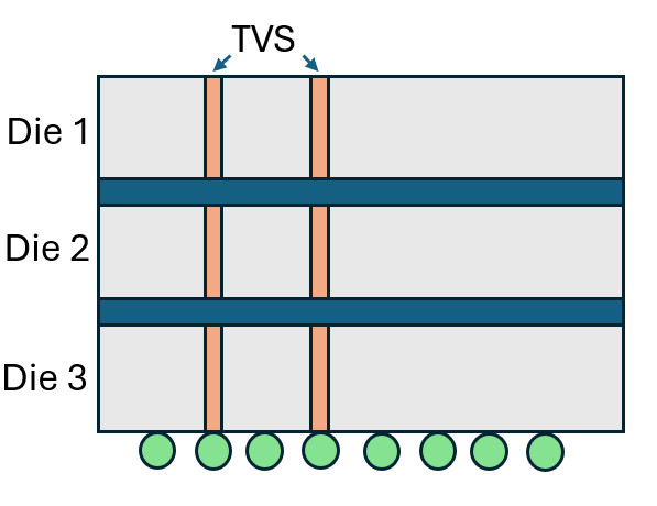
TSVs play a crucial role in 3D integration, a manufacturing strategy whereby integrated circuits are stacked vertically and interconnected by TSVs. By creating vertical connections, TSVs enable a reduction in interconnect length, which minimizes parasitic capacitance and inductance, reducing signal delay and improving overall electrical performance. This is particularly pivotal in devices such as image sensors and stacked memory layers where the proximity of layers directly impacts performance and efficiency. The electrical signals routed via TSVs maintain signal integrity even at high frequency due to the shorter path and reduced susceptibility to crosstalk and electromagnetic interference.
Several key parameters govern the performance and reliability of TSV-based structures, including:
Leveraging these performance factors effectively during TSV design and fabrication is instrumental in optimizing the capabilities and durability of 3D integrated circuits.
The process flow for fabricating Through-Silicon Vias (TSVs) involves several highly technical steps, which can vary depending on the desired application, but typically adhere to a specific sequence to ensure viability and performance. The TSV process includes substrate preparation, via creation, barrier and seed layer deposition, via filling, planarization, and finally, backside processing.
The manufacturing of Through-Silicon Vias begins with substrate preparation, often involving cleaning and the application of an etch mask to define the via pattern. The etching process follows, creating the cylindrical holes that will become the TSVs. This is known as ‘via formation,’ and can use techniques such as deep reactive-ion etching (DRIE) to achieve the desired depth and aspect ratio.
Once the vias are formed, the inner surfaces are prepared to ensure adhesion and prevent leakage current by depositing a barrier layer utilizing chemical vapor deposition (CVD) or physical vapor deposition (PVD). A seed layer is then applied to facilitate the subsequent electrochemical plating process.
Electrochemical deposition (ECD), widely used for via filling, contributes to the fine-grain structure of the conductive material. Planarization, such as chemical mechanical polishing (CMP), levels the wafer surface post-via filling and before the final backside reveal, where the wafer is thinned, and the TSVs are exposed for interconnection to other circuit elements or packaging layers.
Etching of TSVs is primarily achieved using DRIE, a process characterized by alternating etch and passivation steps, which enables control over both the etch rate and profile. Critical process parameters include gas chemistry (typically SF6 and C4F8 gases), chamber pressure, power settings, and substrate temperature. The control over these parameters dictates the etch rate, via sidewall profile, and the potential for scalloping effects. Moreover, high-aspect-ratio etching requires adjustment of these parameters to mitigate factors such as aspect ratio dependent etching (ARDE) and the notching effect.
Deposition within the TSV follows the etching and barrier layer application and is pivotal in forming electrically conductive paths. One commonly utilized method is electrochemical deposition (ECD), which leverages the seed layer to deposit metals, typically copper, within the via. ECD requires parameters such as electrolyte composition, current density, and agitation to be controlled for uniform filling and to avoid voids.
Alternately, for certain applications, physical vapor deposition (PVD) or CVD might be employed, particularly where a conformal coating is essential, though they may present challenges in completely filling high-aspect-ratio vias without voids or seams. The selection of the deposition technique hinges on the via geometry and the desired electrical and mechanical properties of the fill material.
The fabrication of TSVs is completed through several refinement steps, including planarization and backside processing, that prepare the wafer or die for further integration into complex 3D packages. These advanced approaches to integrated circuit design call for precise control of process parameters to meet the stringent demands of modern semiconductor devices.
Through-silicon via (TSV) technology presents a paradigm shift in the field of semiconductor device fabrication by offering significant advantages in the form of increased circuit density, improved electrical performance, and enhanced form factors. TSVs enable vertical interconnect access (VIA), essentially allowing electrical connections to pass completely through a silicon wafer or die, facilitating three-dimensional (3D) stacking of semiconductor devices. This vertical integration overcomes the limitations of traditional planar circuit architectures, leading to shorter interconnect lengths and hence reduced signal propagation times.
Additionally, TSVs play a critical role in heterogeneous integration, where different semiconductor technologies are combined within a single package, promoting functional diversity and system-level enhancements. These benefits have broad implications for various applications, ranging from high-performance computing and advanced mobile devices to specialized sensors and memory stacks.
Key Advantages:
The integration of TSVs into silicon wafers has led to a dramatic improvement in circuit density. By stacking integrated circuits (ICs) vertically, designers are no longer constrained by the two-dimensional plane of the die surface, allowing for more efficient use of space and enhanced circuit integration. This increased density directly correlates to improvements in performance, as shorter interconnects exhibit lower resistance and parasitic capacitance, which, in turn, lead to faster inter-chip communication.
Moreover, TSVs support high current densities due to their vertical structure and the use of conductive materials such as copper, which is known for its excellent electrical properties. By providing a direct path for signal and power transmission, TSVs minimize the path length electrons have to travel, reducing latency and improving overall signal integrity. Significantly, TSV technology also lessens the reliance on slower interconnect methods, such as wire bonds or flip chips, further bolstering IC performance.
Image sensors represent a key application area for TSV technology due to their inherent need for high-speed data transfer and compact form factors. By incorporating TSVs, image sensors can achieve faster readout speeds and reduced noise levels, which are essential for high-resolution imaging applications. The direct vertical connections provided by TSVs minimize the signal path from the photodiodes to the processing circuits, enhancing image quality and sensor responsiveness.
In the realm of circuit boards, TSVs offer a means to achieve denser packaging and improved electrical performance. Traditional surface-mounted technology is often limited by the available board area and the routing complexity for high pin-count devices. Implementing TSVs allows for more efficient board layouts by stacking components and through providing more direct signal routing options, which is particularly beneficial in applications where space is at a premium, such as mobile devices and wearable technology.
TSV technology has undergone significant advancements, particularly in the pursuit of optimal 3D integration solutions. Innovations in TSV fabrication techniques, such as the adoption of high-aspect-ratio TSVs and the development of new barrier and seed layer materials, have expanded the applicability of this technology. Improvements in deposition rates, barrier layer integrity, and the refinement of electrochemical deposition processes for via filling contribute to high-quality, reliable vertical interconnections.
The continued evolution of TSV technology is not only enhancing the performance of individual ICs but is also enabling the creation of 3D packages, which integrate multiple dies into a single, compact configuration. These advancements lead to significant improvements in overall system performance by reducing inter-die communication delays and maintaining signal integrity even at high frequencies. Progress in this domain also addresses critical challenges such as thermal management, leakage current reduction, and mechanical stress minimization, which are crucial for maintaining the integrity and longevity of 3D packages.
As a result of these advances, TSV technology is becoming increasingly pivotal in the semiconductor industry, driving innovation and enabling more powerful, efficient, and compact electronic devices.
Through Silicon Via (TSV) technology, while potent in revolutionizing the semiconductor industry, faces complex challenges that need meticulous attention to ensure the promise of 3D integration is fulfilled. These challenges span from fabrication complications, electrical issues, to mechanical reliability, each of which requires tailored solutions.
Key Challenges:
To address these challenges, semiconductor engineers and researchers have developed a variety of solutions:
Leakage current in TSVs is a significant concern, as it leads to increased power consumption and can cause deterioration of device performance over time. The primary causative factor for leakage current is the diffusion of metal ions from the via into the surrounding silicon substrate.
Barrier Layer Implementation:
To prevent leakage, barrier layers are deposited on the walls of the etched via prior to the filling process. The barrier serves to inhibit metal ion diffusion and ensure the integrity of the TSV. Typical materials for barrier layers include tantalum (Ta), titanium (Ti), titanium nitride (TiN), and tantalum nitride (TaN), chosen for their excellent diffusion blocking properties.
Barrier Layer Challenges:
Recent research focuses on optimizing the deposition techniques, such as atomic layer deposition (ALD), to achieve uniform and conformal barrier layers, even in challenging geometries.
The integration of TSVs can introduce significant mechanical stresses within the silicon substrate, primarily due to the CTE mismatch between the silicon and the materials used for filling the vias, like copper. These stresses can lead to wafer deformation, known as warpage, and in extreme cases, result in microcracks or chip failure.
Residual Stress Analysis:
To prevent structural failures, extensive simulation and modeling are performed to understand the stress distribution and evolution throughout the TSV fabrication process and subsequent thermal cycling. Techniques such as Raman spectroscopy, X-ray diffraction, and finite element analysis (FEA) are employed to measure and predict stress levels.
Stress Management Solutions:
Material innovation plays a pivotal role in enhancing the robustness of TSVs. With conventional materials occasionally falling short in performance or reliability, alternative materials are being explored to fortify TSV structures.
Materials Under Consideration:
Technique Advancements:
By strategically implementing these materials and techniques, TSV technology can continue to advance, fostering the development of ever-more-capable electronic components.
In the dynamic field of semiconductor fabrication, Through-Silicon Via (TSV) technology is positioned at the forefront of 3D integration techniques. Moving forward, several trends and developmental precepts predict the trajectory of TSV technology:
Sensitive to these emerging trends, the semiconductor industry is preparing for a transformation in circuit design and functional capabilities that TSV technology promises to deliver.
Achieving high-performance interconnectivity is at the heart of TSV technology. The goal is to maintain a low resistance-capacitance (RC) delay, ensuring rapid transmission of signals through the vertical connections. Here are some of the latest techniques and innovations:
A list illustrating interconnect techniques:
With these strategies in place, the next generation of TSV-based devices aims to present unprecedented interconnect performance for high-speed applications.
Ensuring power integrity is a critical aspect of TSP technology, and recent advancements focus on maintaining stable voltage levels across all operational modes. In this arena, innovations include:
The planned enhancements explicitly aim to bolster the robustness of the power distribution network within a 3D-integrated system.
The incorporation of III-V compound semiconductors, such as gallium arsenide (GaAs) and indium phosphide (InP), into TSV technology presents an exhilarating frontier. Specifically, these materials exhibit superior electron mobility, which is advantageous for ultra-fast electronics and optoelectronics. The integration of III-V materials could result in:
Research into this domain aims to overcome the challenges of material integration, such as lattice mismatch and thermal expansion difference, to fully harness the potential of III-V semiconductors within the 3D microelectronics ecosystem.
There is a total of three kinds of through silicon vias or TSVs based on the manner they have been manufactured.
Via-first TSVs
This is when the TSV is fabricated before the actual device has been patterned or the metal layers have been laid down.
Via-middle TSVs
This is when the TSV is fabricated after the front end of line process has been completed but before the back end of line part begins, i.e. before the metal layers are put down. This is the most popular method of TSV development and deployment when it comes to interposer stacks and three dimensional integrated chips.
Via-last TSVs
This is when the TSV is fabricated after both the front as well as the back end of lien processes have been accomplished.
TSVs are vertical electrical connections that pass through a silicon wafer or die, enabling 3D stacking of chips. They facilitate communication, power delivery, and data transfer between stacked chips.
TSVs offer several advantages over wire bonding and flip-chip bonding, including:
There are three main types of TSVs:
The main fabrication steps include:
TSVs are widely used in various applications, such as: