

Under-bump metallization (UBM) is a critical aspect of the functionality of Semiconductor devices, forming the crucial connections between integrated circuits and the outside world. This intricate process plays a vital role in ensuring that electronic components operate with precision, particularly in the context of the ever-shrinking size of devices and increasing demands for performance. In this article, we will delve into the technicalities of under-bump metallization, exploring its structure, components, and the methods by which it is implemented. Additionally, we will examine how UBM has revolutionized flip chip bonding, compare it to the traditional wire bonding method, and discuss its impact on the longevity and dependability of electronic packages.
Credit: research gate
Under-Bump Metallization, often abbreviated as UBM, ranks high as a pivotal process in microelectronics. It’s the layer that meticulously connects the semiconductor’s contact pads to its package’s bumps. Primarily used in flip-chip technology, UBM serves as a versatile intermediary, fulfilling electrical, mechanical, and thermal responsibilities. This versatile layer ensures signal integrity, sturdy mechanical bonds, and efficient heat conduction, all crucial in maintaining the chip’s performance and longevity.
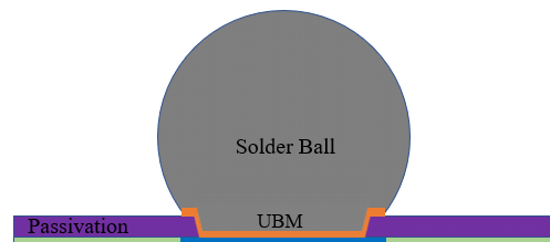
The UBM process adapts to various materials, including aluminum or copper pads, integrating seamlessly with solder bumps composed of lead-tin or lead-free alloys. The typical structure of UBM involves multiple layers, each customized for specific functions—adhesion, barrier, and wetting—maximizing the efficacy of the solder connection.
Implementing UBM in circuit design is a testament to advancing technology’s push towards miniaturization and performance efficiency. It’s a blend of precision engineering and material science that reflects the innovation at the heart of modern electronics manufacturing.
UBM’s role in the formation of electrical connections is both foundational and finely detailed. It acts as the connective tissue between the chip and its carrier, ensuring that the flow of electricity is seamless and stable. The role UBM plays can be dissected into three main functions, each critical to establishing and maintaining reliable electrical connections.
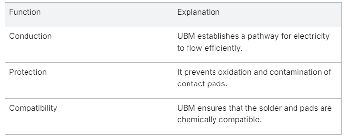
By fulfilling these roles, UBM transforms a potential point of weakness – the interface between chip and carrier – into a point of resilience. It ensures that the electrical connections can withstand the thermal expansion and contraction that often occur during device operation. As devices become more complex and the power running through them increases, the importance of a secure electrical connection cannot be overstated. UBM is the unsung hero in this equation, reliably performing behind the scenes to connect the dots in our technologically driven world.
The architecture of Under-Bump Metallization (UBM) is purposefully designed, comprising multiple thin film layers each serving a unique function within the microelectronic framework. These components, when combined, form a robust, conductive, and protective structure. The precision in UBM construction is essential to achieve the intended electrical continuity and mechanical stability for the integrated circuit’s interconnections.
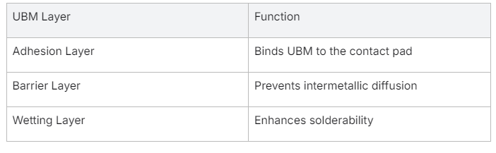
UBM utilizes a stack of layers that can generally be classified into three primary types:
The exact sequence and composition of these layers can vary based on factors such as the device’s performance requirements and the manufacturer’s proprietary processes.
Barrier layers within the UBM have a pivotal role. They are engineered to impede the diffusion of solder and other metal atoms into the semiconductor material. This diffusion can adversely affect the performance and reliability of the device if left unchecked. Common materials for barrier layers include nickel, vanadium, or their alloys, known for their resistance to interstitial diffusion.
The choice of materials for UBM is crucial as they must possess specific electrical and mechanical properties. They often include metals such as:
These materials play specific roles in UBM: aluminum or copper for adhesion; titanium, titanium-tungsten, chromium, or nickel-vanadium for barrier purposes; and silver, gold, or copper for providing a solder-wettable surface.
Adhesion layers are essential to the structure’s integrity as they ensure the UBM layers’ cohesion with the underlying silicon wafer or interlayer dielectrics. Materials like aluminum and copper are frequently chosen for their strong affinity with both the UBM layers above and the layers below, serving to anchor the whole UBM stack firmly in place.
Dielectric layers aren’t a direct component of UBM but play a related role. They electrically isolate the bumps from each other and the rest of the IC structure. Typically composed of materials with low electrical conductivity, such as silicon dioxide or silicon nitride, these layers work hand in hand with the UBM to ensure signal integrity and protection from electrical crosstalk between adjacent bumps.
Creating an effective UBM structure involves precision engineering and careful selection of manufacturing techniques. These processes must accommodate fine geometries and provide the necessary electrical and mechanical properties essential for device functionality.
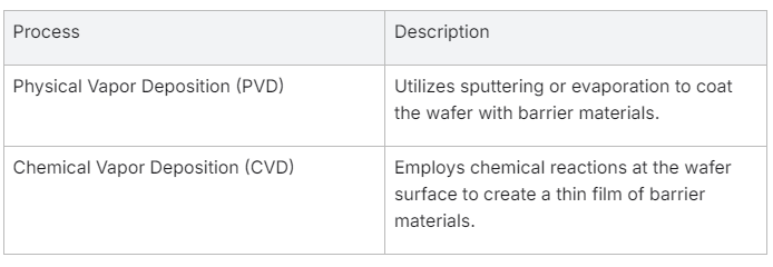
The deposition of the diffusion barrier and subsequent metallization layers are critical components of UBM and are usually achieved through methods such as physical vapor deposition (PVD) or chemical vapor deposition (CVD). In the PVD process, target material atoms are deposited on the semiconductor wafer by physical means, such as sputtering under vacuum, while CVD uses chemical reactions to produce high-purity, high-performance solid materials.
Once the barrier layer is in place, the wettable layer is typically added using electroplating or immersion deposition techniques. Electroplating involves passing a current through a plating solution where metal ions reduce to form a solid metal coating on the wafer. Immersion deposition, on the other hand, is a chemical displacement reaction where a thin film grows on the wafer by immersion in a solution containing ions of the film’s metal.
The integration of UBM in semiconductor devices is the concluding step in packaging where UBM structures are connected to the pads on the device and then to the outside circuitry via solder bumps. This phase also needs to align with the device’s final application regarding scalability, density, and performance criteria. The integrated UBM ensures that electrical signals are effectively communicated from the silicon to the macro-scale of the device’s operational environment, establishing a reliable link between the microscopic and human-scale elements of electrical circuitry.
UBM integration steps include:
Each method and process used in UBM contributes significantly to the integrated circuit’s overall performance, reliability, and lifespan.
Under-Bump Metallization (UBM) plays an essential role in the process of flip chip bonding, a method for direct electrical connections of face-down (or “flipped”) integrated circuits (IC) onto substrates, printed circuit boards (PCBs), or carriers. UBM is the intermediary between the die and the bumps that form the connection points to the substrate. It ensures the formation of a robust mechanical bond and signal integrity between the chip and the external circuitry through a series of metallurgical reactions and diffusion processes.
UBM layers serve multiple purposes: they create a suitable surface for soldering, provide a strong adhesion to the die pad, act as a barrier to prevent inter-metallic compound formation, and protect the silicon during the soldering process. The precise application of UBM is crucial, as it directly influences the yield and reliability of the flip chip assembly.
The main steps used in UBM for flip chip bonding include:
These steps establish the necessary groundwork for high-density connections typical in advanced semiconductor packaging, allowing for the miniaturization and enhanced performance of modern electronic devices.
Flip chip bonding with Under-Bump Metallization offers several advantages over traditional packaging techniques. UBM provides a reliable electrical connection and mechanical support, enabling the construction of more compact and complex electronics with superior performance. Some of the tangible benefits of employing flip chip bonding with UBM include:
Leveraging these advantages, flip chip bonding with UBM supports the development of smaller, faster, and more efficient electronic devices that are better suited for the ever-increasing demands of the technological landscape.
Flip chip bonding with UBM and wire bonding represent two divergent paths in semiconductor device packaging, each with its own set of strengths. The primary difference lies in the connection density: flip chip bonding can accommodate a higher number of connections in a given footprint, making it ideal for applications where space and performance are critical.
The superior performance of flip chip bonding with UBM, however, comes at the cost of complexity; establishing UBM layers involves a series of precision processes that represent a higher initial investment in both equipment and development. Conversely, wire bonding has been a mainstay in the industry for decades, and its relatively simple process translates to lower initial setup costs. Nevertheless, factors like device miniaturization and high-speed operation are driving the industry toward the more advanced approach provided by flip chip bonding with UBM.
The reliability of electronic packages hinges significantly on the robust performance of UBM. Given the constant miniaturization in electronics, the demand for reliable interconnects that can maintain integrity even at reduced sizes is paramount. Poor-quality UBM can lead to a host of issues, such as poor solder wetting, weak joint formation, electromigration, and corrosion—all of which can lead to device failure.
UBM is especially critical in ensuring the mechanical strength of the solder joint against stresses and strains during service life which includes numerous thermal cycles. Each thermal cycle can induce expansion and contraction in the materials, and the UBM must maintain a solid interconnection throughout these fluctuations. Additionally, UBM safeguards against the diffusion of elements that can degrade the connection over time, and thus, plays an essential role in bolstering the overall longevity of the electronic package.
In sum, the effectiveness of UBM in electronic packages is non-negotiable for attaining the high levels of performance and reliability that modern semiconductor devices require. Through the adept application of UBM layers, electronic components can surmount the challenges posed by today’s fast-paced advancements and consumer demands for smaller, more powerful devices.
Numerous factors impact the reliability of Under-Bump Metallization, from material selection to implementation. UBM reliability is contingent upon:
Addressing these factors effectively can greatly enhance the performance and reliability of electronic packages.
Get an indicative packaging cost range, then a detailed breakdown by email.


