

When mobile phones changed into smart phones a proximity (PS) and ambient light sensor (ALS) became an important sensor in every phone. Measurement of ambient light is used to adjust the screen backlight. The proximity sensor is used to detect a person holding to phone near the ear. While some mobile manufacturer chose to combine the sensors (PS and ALS), some prominent mobile manufacturer made the choice to keep them separate.
More than two decades ago in optical storage devices integrated photodiodes were used to convert optical bitstreams into the electronic signal. SystematIC was involved in this domain at a time when the technology was mature and stretched to the limits of mechanical, optical and electrical performance. On-chip photodiodes were combined with low noise, accurate signal processing electronics that were mounted on flex prints.
Experienced in optical storage SystematIC’s first developments in the combined PSALS domain started in 2009 and resulted in a 10bit PSALS chip in a cost effective 0.6um CMOS process. In operation the chip required less than 100uA supply current and in standby this reduced orders of magnitude. The first product was quickly followed by a chip in a 180nm CMOS process which was the start of many generations of PSALS designs in that technology node. The 180nm CMOS appeared to be a sweet spot for this mixed signal IC design. Alongside the PSALS, SystematIC developed ALS chips offering ambience light intensity measurement that matches human eye response under a variety of lighting conditions.
In the market, the combined PSALS sensor has become a commodity with a variety of competitors. Chips appeared with different integrated photodiode structures both in mechanical as well as optical domain to detect RGB and IR wave lengths.
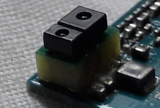
Constant pressure to reduce part cost triggered developments into ever smaller packages and smaller chip size. Application in the modern mobile phones confronts chip designers with challenging requirement to the IC’s. Initially a dedicated area was reserved on the top of the phone’s transparent screen, later the screen became black and almost nontransparent. In the latest generation high end phones, the sensor operates behind an active display. Ambient light rejection during proximity detection and rejection of reflections inside the phone are challenges that are counteracted in the best of class architectures.
SystematIC has developed a set of key IP blocks in 180nm CMOS and supports custom IC developments that covers all of the modern applications. These IP blocks consist of photodiode readout, signal processing, 16 bit sigma delta converters and features and functions in the digital domain. SystematIC cooperates with partners in the product development. Customers have access to technology, proven on silicon, to develop custom products in short development time for their next generation IC’s.
About SystematIC:
SystematIC Design is an analog, mixed-signal IC design and turn-key solution provider company specialized in sensor interface and power conversion topics. We can be a perfect one-stop shop for a company seeing a need of solid ASIC or SoC solution fast and right-at-first-pass.
We provide all design services related to ASIC product development: feasibility study, IC architecture investigation, detailed design and chip layout We also assist in sample evaluation, testing, and application support for which we have our own lab.
We provide full turn-key solutions for customers, that entails us starting from the product idea moving to product development and supporting IC production. Our customers see us as an extension to their product development team. They leverage partnerships with world’s leading manufacturing service providers, while we hold the sole responsibility of the entire supply chain from order to delivery at customers’ manufacturing site.
Over the past 20 years we gained experience in a variety of IC process technologies such as CMOS, Bipolar, BiCMOS, SiGe, SOI and BCD, ranging from high-voltage micron-scale to sub-micron low-voltage. This flexibility, along with a consistent set of analog IP building blocks, allow us to rapidly engage in a new design. Then we rely on our systematic methodologies to attain fully functional, on-spec silicon to serve you: our customer.
Markets served include automotive, consumer and industrial electronics.
Contact:
Richard Visee, CEO
Email: contact@systematic.nl
Website: www.systematic.nl


