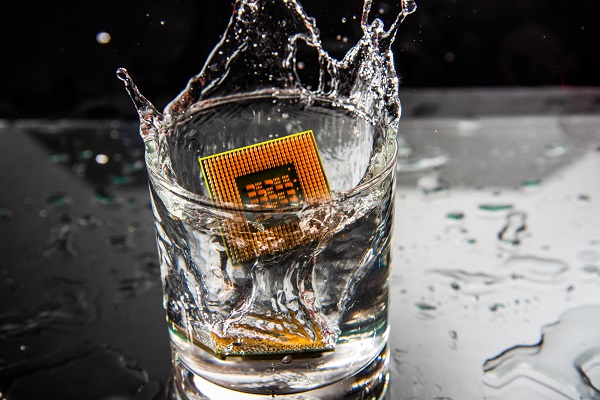
Semiconductor integrated circuits (ICs) are an essential component of every other modern technology which is why they have undergone some of the most extensive growth. Today, IC packaging offering is wide and deep with many kinds and types of semiconductor packaging technologies. Your goal is, therefore, to select an IC package that suits perfectly to your ASIC, not over engineered – because it will increase your IC cost and not under engineered – because it could hurt your IC performance.
With the available variety, it can be difficult to determine what kind of IC package would best suit your needs and support your application ideally. You must take into consideration several different factors such as power, connectivity, application, costs, assembly capability, etc. Let’s further explore each of these various key elements.
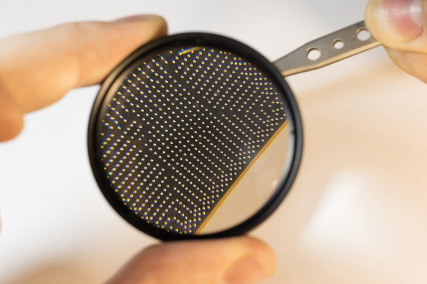
Number of I/Os
This is an essential step when selecting your IC package. You want to lay down the specific groundwork dictating the number of input and output pins you need as well as the location of each pin on the target ASIC.
Tip: BGAs are ideal for high pin counts while it is recommended that you go for a QFN package or WLCSP if you are looking for a lower pin count.
Heat Management
Overtime, the physical size of an average semiconductor IC has gone down while its capabilities have become larger in capacity as well as much faster. As such, it is only understandable that it produces a significant amount of heat – which is why you have to consider the issue of heat management when deciding on your ASIC package. You want to make sure that you chip is operating within the optimum temperature range otherwise you might end up causing irreparable failures.
Tip: BGAs tend to be employ effective heat dissipation methods such as built in metal lid and conductive vias. QFN packages are smaller in size and use a metal exposed pads at the base of the package for this purpose are ideal for low power applications.
High Speed I/Os
You want to make sure that the interconnections in your package do not hamper down the quality of the input and output signals to your IC. You can, for example, choose whether you want bumping technology, which allow you to reach higher frequencies with lower inductance, or wire bonds, which enable you to use lower frequencies but will randomly variable inductance at each RF input and output. The layout of the package also dictates the integrity of the signal as it travels on the surface of the conductor and so the assembly of the board plays an important role in its transmission characteristics.
Tip: If you are looking for high frequency signals upwards of 5 GHz, then you should consider bumping technologies such as flip chip BGA, WLCSP or eWLB.
PCB Assembly
PCB assembly basically dictates how your IC is actually connected to the circuit board. You must give this some thought beforehand as there are multiple methods of doing so that you can choose from. You must also consider the fact that not every provider offers every method, so you might have to look for someone who does what you require. If you are opting for wafer level packaging, or bare die assembly, that has a small pitch (distance between the solder balls) then you will have to go to a service that can conduct this rather complex process and have adequate resources.
Environmental
You must also think about the environment requirements that your IC be exposed to and the effect it may have on its longevity and performance. This will dictate the kind of material you use for the chip and the housing. You may have to use a ceramic or hermetic metal housing if you must protect it from moisture or chemical agents such as in the medical industry. Those involved in automotive must ensure that their packages can resist high temperatures, vibrations, and shocks derived from their environment.