
In a world hungry for efficient power, Silicon Carbide Semiconductors are the unsung heroes behind the scenes. From revolutionizing industrial machines to powering sophisticated electronics, their impact is both broad and deep. Prepare to discover the versatile applications that make silicon carbide semiconductors a cornerstone of modern technology.
This article is your portal to the future as we explore the crystal growth processes that cultivate the potential of silicon carbide and the substrates that serve as a foundation for innovation. As we dive into their role in power electronics and the advancements propelling this technology forward, prepare to be at the forefront of an electrical revolution.
The SiC device market, valued at around $2 billion today, is projected to reach $11 billion to $14 billion in 2030, growing at an estimated 26 percent CAGR (Exhibit 2). Given the spike in EV sales and SiC’s compelling suitability for inverters, 70 percent of SiC demand is expected to come from EVs. China, where anticipated EV demand is highest, is projected to drive around 40 percent of the overall demand for SiC in EV production. (source: McKinsey)
SiC power devices will soon represent 30% of the overall power device market – in the next 5 years. Without doubt, the SiC industry (from crystal to modules, including devices) has a very high growth rate. Yole Group estimates that billions of $ are invested in both crystal and wafer manufacturing as well as device processing, with a market potential of $6 billion by 2027, up from around $1 billion in 2021.

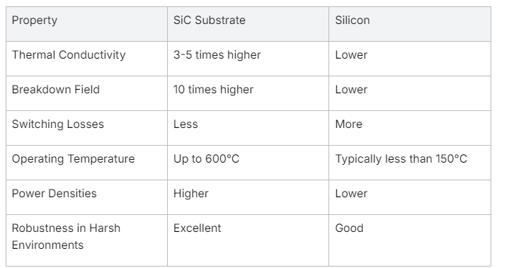
Silicon carbide (SiC), a compound semiconductor, has emerged as a pivotal material in the semiconductor industry. Its advantageous physical and electronic characteristics not only facilitate the design of devices with superior performance metrics but also catapult the reach of semiconductor technologies into realms previously unattainable with traditional silicon semiconductors. In particular, SiC’s exceptional thermal conductivity, which significantly outpaces that of silicon, enables it to operate at elevated temperatures and power densities with improved efficiency and reliability. Additionally, the compound exhibits a higher breakdown voltage and lower switching losses which translate into high-current handling at reduced voltage drops. Owing to these attributes, SiC semiconductors are redefining power electronics, presenting substantial gains in efficiency and thermal management.
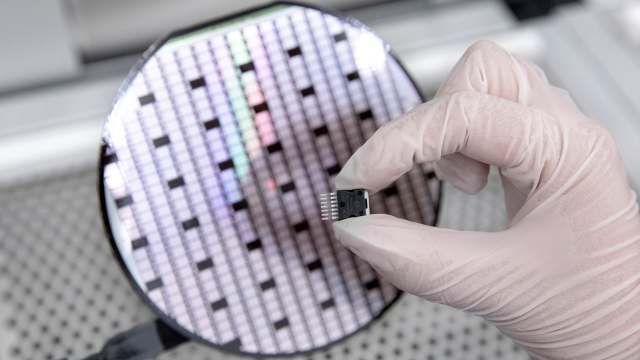
Image source: Bosch
In the context of industrial applications, SiC power devices have become instrumental due to their adeptness in handling high-power applications where efficiency and thermal stability are paramount. For instance, SiC is incorporated in power conversion systems that necessitate high breakdown voltages and low switching losses, resulting in a considerable uptick in overall system competence. Furthermore, these semiconductor devices are increasingly preferred in motor drives, renewable energy inverters, and smart grid infrastructure due to their significant reduction in energy loss and capacity to sustain intense electrical fields and current densities. The robustness of SiC substrates has proven instrumental in scaling up these applications to handle mass production while maintaining consistency and reliability.
In the realm of electronic applications, SiC semiconductors are revolutionizing the landscape with devices that showcase remarkable resistance to thermal degradation and boast high breakdown fields significantly higher than traditional materials. This manifests in enhanced performance for power components in electric vehicles (EVs), where higher power densities and thermal conductivity translate into improved range and reliability. SiC technology is not just restricted to power-based scenarios; the material’s high-frequency operation capabilities also make it ideal for RF (radio frequency) and microwave applications, promising improved efficiency for telecommunication devices.
Furthermore, advancements in SiC crystal growth and processing have led to the development of substrates with superior surface qualities, essential for the fabrication of high-purity semiconductor layers. Through methods such as thermal annealing, the conductivity of SiC can be fine-tuned to create n-type or p-type semiconductors, pivotal for precision electronic devices. The advent of larger substrate sizes, such as 8-inch SiC substrates, signals the semiconductor industry’s commitment to scale up the adoption and integration of SiC technology, ensuring its position as a cornerstone in the future landscape of power electronics and beyond.
—
Silicon carbide semiconductors, often denoted as SiC, represent a class of wide bandgap and compound semiconductors with remarkable physical properties. With a bandgap approximately three times larger than that of silicon, SiC is inherently able to operate at high voltage levels and temperatures that would compromise silicon-based devices. Its crystal lattice structure confers it exceptional thermal conductivity, approximately thrice that of silicon, facilitating heat dissipation and enabling devices to function efficiently under thermal stress.
In addition to thermal robustness, SiC exhibits a breakdown electric field that is significantly higher than silicon, giving it the ability to endure stronger electrical fields without undergoing breakdown. This property is critical in applications that demand high-power delivery and fast switching capabilities with minimal switching losses. SiC’s ability to accommodate higher current densities compared to silicon contributes a further edge in miniaturized yet powerful devices.
Moreover, SiC semiconductor technology is notable for its high electron mobility, conducive for high-speed switching, and the ability to attain saturation velocity swiftly, making it well-suited for high-frequency applications. It’s the amalgamation of these advanced attributes that underpin SiC’s superiority, setting it apart as an advanced material poised to shape the future of semiconductor devices.
Within the semiconductor industry, SiC has risen as a transformative substance, poised to address the proliferating demands for efficiency and performance which have outstripped the capabilities of conventional silicon-based technology. Its compatibility with existing semiconductor fabrication processes, combined with the ability to meet stringent requirements for power, frequency, and thermal management, has cemented its role within the industry.
SiC semiconductors are witnessing expansive growth, driven by pressing needs for energy-efficient power electronics, robust performance in harsh environments, and miniaturization of components without sacrificing power or thermal efficiency. The industry is progressively advancing toward wider adoption of SiC, with key players investing heavily in the production of SiC substrates and devices reflecting its growing importance in cutting-edge applications.
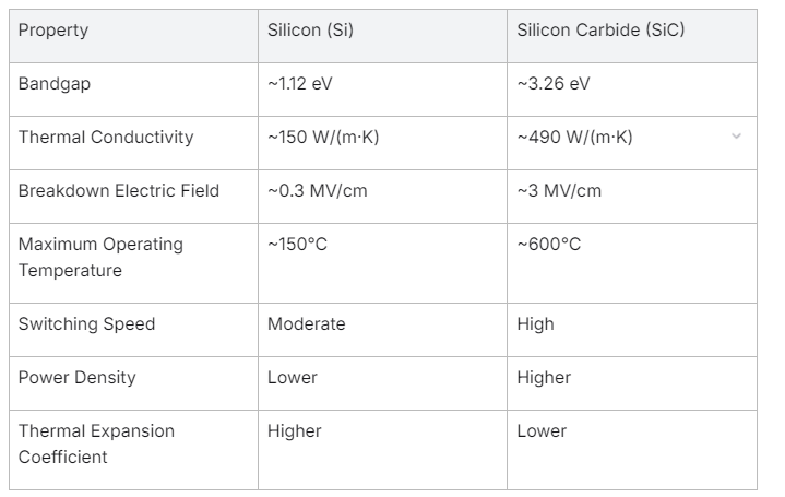
Traditional silicon semiconductors, the industry stalwarts, have seen widespread utilization due to their ease of manufacturing and low material costs. However, their lower bandgap energy and thermal conductivity impose restrictions on performance at high temperatures and high power densities. Comparatively, SiC semiconductors provide enhanced options by offering elevated breakdown voltages, higher thermal conductivity, and superior thermal stability. Such comparative advantages empower SiC-based devices to operate more efficiently, at higher frequencies, and in more challenging environments than their silicon counterparts.
Compound semiconductors like SiC are constituted of more than one element, which in the case of SiC, is silicon and carbon. Unlike single-element semiconductors (e.g. silicon and germanium), compound semiconductors feature varied atomic bonding characteristics resulting in diverse electronic and optical properties. These properties, such as higher electron mobility and direct bandgap, make compound semiconductors particularly useful for optoelectronics, high-speed, and high-power devices.
The significance of compound semiconductors is accentuated by the increasingly demanding electronic applications that require superior speed, efficiency, and functionality not achievable by traditional single-element semiconductors. Consequently, materials like SiC are at the forefront, underpinning innovations in renewable energy, automotive electronics, communications, and defense systems. The trajectory of SiC and other compound semiconductors points toward a future where they play a pivotal role in the further advancement of electronic and photonic technologies.
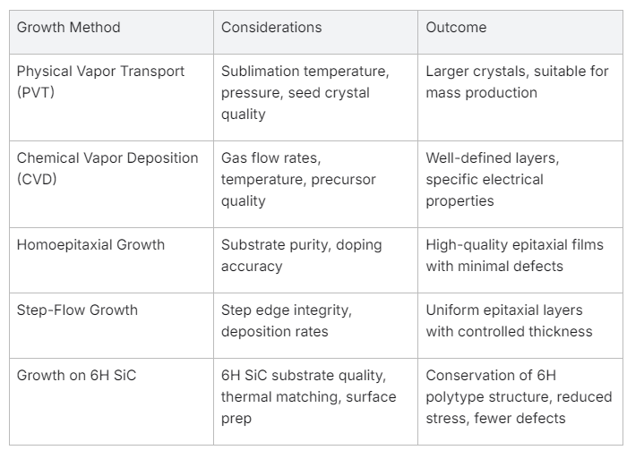
The production of high-quality silicon carbide (SiC) crystals is fundamental to the mass production of SiC semiconductor devices. The growth technique chosen influences the final quality of the SiC substrates, which is crucial for achieving the desired electronic properties in devices. Crucial to this process is maintaining the integrity of the crystal structure, minimizing defects, and achieving desired doping levels and homogeneity. Two primary methods for crystal growth dominate the industry: the Physical Vapor Transport (PVT) method and the Chemical Vapor Deposition (CVD) method. In PVT, SiC crystal growth occurs through sublimation of a silicon carbide source which is then re-condensed in seed crystal form. In contrast, CVD relies on chemical reactions of gas-phase precursors to deposit a crystalline layer on SiC substrates.
The growth mechanism of SiC crystals involves a series of complex steps, beginning with the nucleation phase where small crystallites form. These crystallites serve as the foundation for further crystal development. During the growth phase, atoms or molecules from the gas or vapor phase are incorporated into the lattice of the growing crystal. This transition from vapor to solid phase must be carefully controlled to maintain the desired crystal orientation and purity. The rate of addition of new layers to the crystal structure depends on various factors such as temperature, pressure, and supersaturation of the growth environment.
Homoepitaxial growth refers to the epitaxial layer growth on a substrate of the same material. In the case of SiC, this involves depositing crystalline SiC layers on existing SiC substrates, typically employing CVD. Homoepitaxial growth is essential for creating layers with specific electrical properties, determined by the controlled introduction of dopants during the deposition process. This technique aligns the new epitaxial layer with the underlying crystal lattice, resulting in high-quality films with fewer defects and superior semiconductor characteristics.
Step-flow growth is a precision-driven facet of the homoepitaxial process where atomic-scale steps on the substrate surface serve as the key sites for material attachment. Atoms or molecules from the growth environment preferentially adhere to these step edges and then spread laterally to form new atomic planes. This method is most effective when the angle of the growth steps to the substrate surface is optimum for mass transport across the surface, promoting a uniform epitaxial layer. The step-flow technique minimizes defects and is utilized in the homoepitaxial growth of SiC to enhance crystal quality by leveraging the natural step patterns present on the substrate surface.
The 6H polytype of SiC is a specific hexagonal crystal structure that is frequently used as a substrate for epitaxial layers. Growth on 6H SiC requires precise control of conditions to maintain the polytype structure and achieve the desired electronic characteristics. The lattice and thermal match between the epitaxial layer and the 6H substrate are instrumental in reducing stress, defect formation, and ensuring superior electrical performance. Researchers and manufacturers focus on optimizing the quality and size of 6H SiC wafers, affecting yield and performance of SiC power devices. Techniques such as thermal annealing and meticulous surface preparation play pivotal roles in enhancing the 6H SiC growth process for industrial applications.
Table: Procedures and Considerations in the Growth of SiC Crystals
List: Factors Influencing SiC Crystal Growth Quality
The fine-tuned growth of SiC crystals is a cornerstone of the semiconductor industry as it strives to meet the escalating demands for SiC devices in high-power applications. Through meticulous control and innovation in crystal growth techniques, manufacturers continue to advance the scalability and consistency of SiC crystal quality, reinforcing the material’s critical role in the future of power electronics.
Silicon carbide (SiC) substrates have emerged as the foundation for the next generation of semiconductor devices, offering compelling advantages over traditional silicon counterparts. These substrates are constructed from the compound semiconductor SiC known for its remarkable material properties, such as outstanding thermal conductivity, high current density, and superior breakdown voltage. SiC substrates also boast an impressive breakdown field, which significantly enhances their performance under high-power and high-temperature conditions. Additionally, their ability to operate at elevated voltage levels with reduced switching losses is particularly attractive for power electronics.
SiC substrates serve as the critical base material upon which layers of SiC are epitaxially grown to form electronic devices. A critical aspect of SiC substrates is their crystallographic orientation, dopant concentration, and purity, which directly impact the semiconductor’s efficiency and capabilities. As a compound semiconductor, SiC substrates can be either n-type or p-type, depending on the dopants used in their manufacturing process. The enhanced thermal conductivity of SiC allows for better dissipation of heat, fostering higher power densities in electronic devices. The strength and chemical inertness of SiC make these substrates ideal for harsh industrial applications. Furthermore, their lower voltage drop compared to silicon enhances energy efficiency.
The pursuit of larger diameter SiC substrates, such as 8-inch wafers, represents the industry’s drive towards economies of scale and cost-effective mass production. The evolution from smaller substrate sizes to 8-inch SiC substrates significantly impacts the semiconductor industry by permitting more extensive circuits and higher device yield per wafer. With larger substrates, manufacturers can achieve a greater output with each batch of production, thus lowering the cost per device. Producing high-quality 8-inch SiC substrates involves mastering the technical challenges of maintaining consistency across a large substrate surface. The transition to 8-inch SiC substrates plays a vital role in enabling the mass adoption of SiC in sectors demanding high-power electronics.
Table: Advantages of SiC Substrates Over Silicon
List: Benefits of 8-inch SiC Substrates
As the semiconductor industry advances, SiC substrates, particularly those of larger diameters, are poised to play an increasingly fundamental role in shaping the landscape of power electronic applications.
In the realm of power electronics, SiC devices are taking a dominant role, eclipsing traditional silicon semiconductors in applications where efficiency and performance matter most. These devices exploit the unique properties of silicon carbide to accommodate higher voltages, frequencies, and temperatures, positioning themselves as the backbone for a myriad of electronic applications, from industrial motor drives to electric vehicles and grid infrastructure.
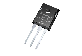
SiC power devices, such as Schottky barrier diodes (SBDs), MOSFETs, and IGBTs, are redefining efficiency and reliability standards. Thanks to the intrinsic material characteristics of SiC, such as its wide bandgap, high thermal conductivity, and exceptional electron mobility, these devices can function at much higher junction temperatures with lower on-resistance. Consequently, this leads to reduced energy waste and a remarkable increase in system-level performance.
|
SiC Device Type |
Benefit |
|---|---|
|
SBDs |
Lower forward voltage, reduced switching losses |
|
MOSFETs |
High frequency operation, reduced on-resistance |
|
IGBTs |
Higher breakdown voltage, efficient high-temperature operation |
Switching losses are a significant concern in power electronics as they contribute to heat generation and impact overall system efficiency. SiC power devices substantially cut these losses due to their aptitude for high-speed switching without compromising performance. Their exceptional breakdown field allows for designs with a much thinner drift region, which not only reduces on-state resistance but also diminishes capacitance, leading to quicker switch-off times.
SiC-based semiconductor devices embody high power density capabilities. Given their ability to efficiently handle high temperatures and dissipate heat, SiC devices enable power electronics to operate at elevated power levels without the need for cumbersome cooling systems—a factor that drastically enhances power density. SiC’s thermal properties thus play a pivotal role, offering a power density up to ten times greater than that of traditional silicon-based devices.
Current density reflects the current carrying capability per unit area of the device, and SiC devices excel with significantly higher current densities compared to silicon. Leveraging superior thermal performance and wide-bandgap characteristics, these devices ensure stable operation under high current scenarios, mitigating the risk of thermal runaway. This attribute is indispensable for high-power applications that demand reliability under stringent conditions.
The voltage drop across a power device is a critical factor in determining power efficiency. SiC devices inherently exhibit a reduced voltage drop, owing primarily to their low on-resistance and quick switching capabilities. Such a significant reduction in voltage drop directly translates into higher electrical efficiency and favours the miniaturization of components, which is crucial for developing compact and energy-efficient power electronic systems.
Efforts to minimize electric power loss are essential for the transition to more sustainable energy practices. SiC’s exceptional proficiency in reducing switching losses, enhancing power density, and sustaining high current densities makes it an optimal candidate for such improvements. The deployment of SiC power devices is identified as a transformative step towards the profound reduction of electric power loss in modern electronic systems, paving the way for innovative designs and eco-friendly technology solutions.