

The continued growth of the mobile handset, tablet, and networking markets requires ongoing development of innovative packaging technologies. The required solutions must provide reduced form factor and high thermal and electrical performance as well as increased functional convergence and system integration. To meet the extremely small interconnect feature sizes in complex designs, especially those with less than 5 µm/5 µm line and space (L/S) trace features, more complex and sophisticated packaging technologies are needed.
The limited scalability of traditional organic and inorganic substrate technologies provides insight into the problem. Organic laminate technologies are currently constrained to 10 µm/10 µm L/S for trace circuity. Conventional wafer-level fan-out (WLFO) designs can achieve 5 µm/5 µm L/S but are limited to one or two metal layers due to the topology challenges in photo imaging a molded wafer. Although silicon interposers can easily provide less than 2 µm/2 µm L/S interconnect densities, the inherent cost impact and supply chain limitations of the through silicon via (TSV) process often makes this an unrealistic option. The end result is an interconnect gap in the 2 µm – 5 µm L/S range, as shown in Figure 1.
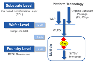
Figure 1. IC Package Integration Roadmap
To close this gap, a new approach to high density fan-out (HD-FO) semiconductor packaging technology has been developed. Silicon Wafer Integrated Fan-out Technology (SWIFT™), also called chip last HD-FO, incorporates the fine feature size capabilities of wafer-level packaging (WLP) coupled with the advanced flip chip packaging technologies, such as chip on wafer (CoW) and Package-on-Package (PoP).
Target applications for this packaging technology include application processors, baseband (logic+memory), and power management units for advanced mobile applications and high-speed switches for network servers.
Figure 2 illustrates the SWIFT assembly process flow.
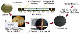
Figure 2. The SWIFT (Chip Last HD-FO) Process Flow
HD-FO incorporates the use of a carrier and thin film photolithography to pattern the fine metal and dielectric features in a multi-layer redistribution layer (RDL) structure. A chip last process has the advantages associated with conventional organic substrates regarding yield and cycle-time. Once the SWIFT (chip last HD-FO) package RDL is fabricated on the carrier, the structure is inspected, known bad RDL sights are identified, and the HD-FO “substrate” is placed in inventory.
This approach enables a shorter overall cycle time and ensures that a known good die is dedicated to a known good substrate. With “chip first” wafer fan-out technologies, where the RDL process is responsible for the majority of the yield impact, this is not possible. The SWIFT approach also has superior flexibility and scalability, since it can support many package variants, such as 3D PoP, system in package (SiP), multi-dies, passive components, and variable component thicknesses.
benefits OF SWIFT PAckaging
With its fine feature and thin stack-up capabilities, the primary benefits for SWIFT packaging include:
Mechanical benefits from this new packaging approach occur in both form factor and feature size. One of the significant benefits of using wafer level packaging is the form factor reduction including the package z height. Package thickness has critical effects on the signal and power integrity since the conductive path changes as the package height changes. In addition, the thermal performance of the package also benefits from a thinned package since the resistive path would be lessened. HD-FO packaging is approximately 40% thinner compared to competing laminate-based technologies and thus shows substantial improvements. Figure 3 shows a comparison of a flip chip PoP vs a SWIFT design cross section where a total package thickness of 450 µm is achieved with SWIFT design vs a flip chip PoP package with a thickness of 630 µm (excluding the memory package).
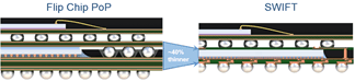
Figure 3. Package Height Comparison with Cross Section View of a FC PoP Package and the SWIFT Package
The SWIFT design builds on conventional WLFO technology and provides improvements to the shortcomings of the limited line width, spacing, and 3D capabilities. With the unique structure of the SWIFT package and the use of key assembly processes such as stepper photo imaging, this technology enables line width and spacing down to 2 µm. This increases the I/O count and circuit density within a reduced area for single and multi-die applications. These fine feature capabilities avoid the 2.5D TSV connections that are typically required for SoC partitioning and networking applications. Multi-layer (up to 4 layers) RDLs can be built with fine (≥ 2 µm) line width and spacing and polymer-based dielectrics providing a single body construction compared to standard flip chip technologies.

Figure 4. Key Enabling Chip SWIFT Technologies
Although the overall package structure resembles a traditional flip chip stack, the use of fine pitch micro bump die interconnects with 30-mm pitch capability and reduced layer count in SWIFT packaging offers key improvements. Figure 4 shows an image of the RDL capability and fine pitch micro bump die interconnects.
The flexibility of the SWIFT package structure also offers benefits for creating 3D assemblies. Tall Cu pillars can be used to create high-density vertical integrations which enable 3D/PoP-like structures where the advanced memory chips can be mounted on top of the package. Figure 5 shows the tall Cu pillars (>200 µm pillar height) and a cross-section picture of a 3D PoP SWIFT design in a dual-die structure with a top RDL.
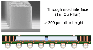
Figure 5. SWIFT Package with Tall Cu Pillars and Top RDL
In addition to these mechanical, system-level packaging advantages, the SWIFT (chip last HD-FO) design methodology has been demonstrated to provide benefits in other areas, including:
These results have been verified through SWIFT test vehicles compared to Exposed-Die PoP and Fan-In PoP products [1]. The SWIFT PoP structure has passed industry-standard component level and board-level reliability requirements. In comparison to a traditional 3D fan-in PoP structure for logic and memory device integration, SWIFT technology exhibits enhanced electrical signal integrity, superior impedance matching, optimized power distribution, and improved thermal performance.
Next Generation Packaging Technology
Compared to incumbent packaging technologies, SWIFT or chip last HD-FO design is a highly integrated structure that has exceptional electrical, mechanical, and thermal performance benefits to meet the needs of next generation mobile, high performance graphics, and network applications. By incorporating the advanced feature size and thin film dielectric benefits of wafer level packaging coupled with the device integration capabilities of flip chip assemblies, SWIFT technology bridges the gap between TSV and traditional wafer level fan-out packages.
The chip last HD-FO technology also has attractive extensions into SiP applications by enabling impressive reductions in package volume and the ability to incorporate innovative EMI shielding techniques. In addition, the technology’s high density fan-out capabilities combined with conventional substrate technology open up opportunities for deconstructed logic integration for network switch applications. SWIFT design methodology is truly a versatile, high performance packaging approach for next generation mobile and network devices and is positioned to serve the semiconductor industry for many years to come.
REFERENCE
[1] B. Baloglu, G. Scott, and C. Zwenger, “Silicon Wafer Integrated Fan-Out Technology,” International Wafer Level Packaging Conference (IWLPC 2017), Oct 18-20, 2016.
Want to read more on SWIFT technology? click here.


