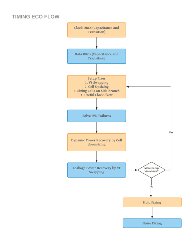
Timing ECOs refer to last mile timing and DRC fixes before you tape-out the ASIC. EDA implementation tools (with help of physical design engineers) do 95-98% of the job when it comes to meeting the timing goals. For the last 1-2% timing violations, however, it is prudent to handle them manually in a more deterministic manner rather than pushing the EDA tools- which may take a longer time to converge, if not entirely give up! Designers need to give a great deal of thought while doing these timing ECOs, in particular, the order in which they should go about fixing the problems. Here’s the recommended order:
- DRC/DRV Fixing: Design Rule Checks (DRCs) or Design Rule Violations (DRVs) usually refer to max_transition and max_capacitance limits set either by the timing libraries, or some tighter values explicitly defined by the designers. We need to fix these to prevent any extrapolation while computing the cell delays from the look-up tables in the timing libraries where the EDA vendor doesn’t guarantee the delay numbers reported by the timing or optimization tools.The first and the foremost fix to start with is the clock fixes. The reason being any changes on the clock path will impact your data path timing by changing the setup or hold windows. Among clock fixes, you can choose to fix clock max_capacitance first or clock max_transition Fixing one would invariably fix the other. Also note that going with the library limit for max_capacitance or max_transition might result in increased internal power dissipation, and designers usually tend to decide on the max_transition limit based on the basis of a certain percentage of clock period, say, 10%.
Transition violations can be fixed by either by upsizing the driver, or perhaps splitting the net by insert a buffer which would effectively split the load driven by a cell and hence improve transition. Buffer insertion would also help fixing max_capacitance violations as well.
After clock DRV fixing, you can perhaps do a data DRC/DRV fixing.
- Setup Fixes: There are many different ways you can fix setup.
- Vt swapping: Swapping the higher Vt (threshold voltage) cells to lower Vt cells can help reduce the delay, at the expense of higher leakage power.
- Upsizing the cells: Upsizing the cells might also help in improving the delay of cells along a timing path, however, one needs to be cautious. If you upsize an x1 cell to let’s say an x12 cell you run into the risk of increasing the load on the previous cell, thereby degrading the overall timing path. This can also result in local IR drop issues as well, because bigger cells would tend to draw more current from the power grid as compared to the smaller cells.
- Sizing cells on the side branch: If you have one cell driving let’s say 3 cells and out of these 3 cells, you have positive setup slack on 2 branches (side loads), while at least 1 fan-out is violating setup, you can try to downsize the cells along the branches with positive setup slack. This will reduce the loading on the buffer, and thereby help improve setup timing on the first fan-out as well.
- Useful Clock Skew: This elongates the window for signal arrival by pushing the clock to the capturing sequential. This method may create hold violations on the same capturing flip-flop, or perhaps even setup violations on the path originating from the capture flip-flop.
- Power Recovery: There are a couple of ways you could attempt to recover power by either
- Downsizing the cells to save dynamic power.
- Swapping the lower Vt cells to higher Vt cells to save leakage power.
Before you even proceed with power recovery, you need to obtain the list of cells failing IVD (Instantaneous Voltage Drop) or dynamic IR drop. One would need to first downsize the cells in the vicinity of the IVD failing cell before attempting dynamic or leakage power recovery because of 2 reasons:
- IVD failure is a must-to-fix check because it can result in timing failures on silicon, while dynamic/leakage power recovery is a good-to-have check because it makes your device dissipate lesser power. You would want to start with a fix that’s more critical.
- More importantly, if you go about downsizing cells to recover dynamic power first, you eat up all the positive slack in your timing paths. Subsequently, if you downsize cells failing IVD, you would see a surge in your timing violations and it will be very difficult to fix these timing paths again.
Therefore, ideal approach is to do downsizing cells in the vicinity of IVD failing instances, and then downsize the cells along a timing path if you still have a positive slack, or else upsize the cells along the timing path if you are violating setup.
Now back to power recovery. Among downsizing and Vt swapping, which one would be better to do first? The answer may vary from design to design, may depend on your overall PPA (Power, performance and area) goals and the technology node you’re working on. However, generally speaking, it’s better to do downsizing first followed by leakage recovery. The reason being swapping the cells to higher Vt would again eat up most of the positive slack in your SoC design, leaving minimal or perhaps no room for further downsizing. And there’s not much difference in the delay of X3 and let’s say X5 cells, it’s just that x5 will be able to drive a longer distance with a sharper (quicker) transition.
- Hold Fixing: The explanations needed here. You can fix hold by inserting buffer at common point or at the endpoint. Former approach would result in optimal number of buffers needed to fix hold timing, but may or may not impact setup timing. The latter approach would result in more number of buffers being inserted but the hold fixing rate would be more predictable and deterministic with possibility of setup degradation being minimal. Another approach could be downsizing or Vt swap, provided you have plenty of setup slack available along the paths failing hold time.
There could be some cases where the same path is both setup and hold critical. While such cases are rare, they do pop up in the design. Such cases need more careful study at very early stages in the design cycle, and many techniques have been proposed to fix timing on such paths, but it’s discussion would be beyond the scope of this post.
- Noise Fixing: Noise fixing should always be the last step in your Timing ECO cycle. Noise is very volatile, and SoC designers cannot afford to fix noise at each and every step. Unless there’s something wrong systematically or there are tons of noise violations that designers may need to analyze which may require designers to re-visit their physical implementation, noise fixing should be done at the last. Any ECO changes- cell upsizes, Vt swaps, buffer insertions alters the timing windows and changes the noise picture. To decrease the number of iterations on fixing noise, it’s most pragmatic to do it at the last.
Last thing to note here is that a single iteration of timing ECOs can potentially degrade some other metric, however, only slightly. For example- if you are fixing setup violations by upsizing the cells you might see a slight degradation in your hold timing, and that’s expected. One might need to do multiple rounds of the above mentioned fixes, and as long as you’re converging in the right direction, timing ECOs are doing their job!
Now that you’ve fixed all timing violations, apparently meeting your Power, Performance and Area targets, you’re ready for tape-out!