

Modern ASIC chips are highly complex and contain millions of transistors, thus, the likelihood of having an error somewhere in the chip during the design process is very high. The earlier the error is detected, the less it will cost. Therefore, ensuring the ASIC is bug free as early as possible, preferably during the design process is extremely important.
The goal of ASIC verification is to make sure that the design meets the system requirements and specifications.
ASIC verification process is one of the crucial things during ASIC design process and can consume as much as 70-80% of the total ASIC design and verification time. Luckily, there are many tools and processes that can help with this task.
Depending on whether the ASIC verification takes place during the design process virtually, using simulations or on a real silicon there are two types of ASIC verifications: Pre silicon verification and post silicon validation.
There are different steps to ASIC verification like logic simulation/emulation and circuit simulation, when detailed functionality and timing of the design are checked using simulation or emulation; functional verification, when functional models describing the functionality of the design are developed to check against the behavioral specification of the design without any detailed timing simulation; formal verification, when the functionality is checked against the “golden” model. Formal verification also consists of model checking, when the model of the design is checked against some presumed “properties” specified in the functional or behavioral model (for example, finite state machine should not enter a certain state), and equivalence checking, when the functionality is checked against the “golden” model. According to late A. Richard Newton there are three main motivations for the verification:
(1) During specification: “Is what I am asking for what is really needed?”
(2) During design: “Have I indeed designed what I have asked for?”
(3) During testing: “Can I tell intact circuits from malfunctioning ones?”
From these questions that can describe two distinct circuit qualities:
Functionality, which describes what responses a system shows at the output when presented with given stimuli at the input. In the context of digital ICs, engineers tend to think of logic networks and of package pins but the concept of input-to-output mapping applies to information processing systems in general. Functionality can be modeled using mathematical concepts like algorithms, equations, impulse responses, tolerance bands for numerical inaccuracies, finite state machines (FSM), and the like, but often also informally.
Parametric characteristics, on the other hand, are related to physical quantities measured in units (for example, Mbit/s, ns, V, μA, mW, pF, etc.) that help to express electrical and timing-related characteristics of an electronic circuit.
There are different types of ASIC chips: Analog, Digital and Mixed Signal. Depending on the type one will have different design workflows and tools used during the design process. However, there is a generic ASIC design and verification workflow shown below.
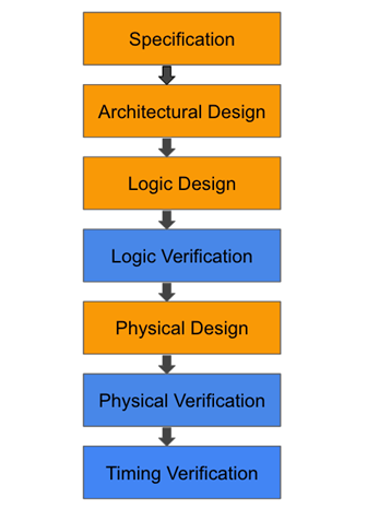
Figure 1: ASIC design and verification workflow
One can see that a verification phase takes place after each step. Depending on the verification result we move to the next step or go back to the previous one. For example, if the logic verification passes without errors, we move to physical design otherwise repeat logic design again until it passes the verification process. If we can’t pass the verification after by changing logic design, we might need to go back to architectural design or check whether the specification is right. If we fail with Physical or timing verification usually, we fist go back and correct physical design. If it doesn’t work, we go back to logic design and so on until it starts working or we make sure that we can’t meet the specification requirements with that technology for example. Simulation based techniques are the most popular ones, even though they are time consuming and can even be imperfect in finding errors and failures in the design. As we can see there are two main types of ASIC verification: functional and non-functional. Functional verification is done using functional models, while non-functional verification is done using the architecture, placement, routing, timing and other parameters of the components of the ASIC.
Digital ASICs are more common in the industry. In the digital design process a hardware verification language (Verilog, VHDL) and standard cell libraries are used.
After RTL code is written, it should be checked to make sure that it works as expected (functional verification) before the synthesis. So basically, verification goes in parallel with the design. Typically, a verification engineer reads the hardware spec, creates a verification plan and follows it to build tests to see whether the RTL works correctly or not.
The test then is run on the RTL code to see if design matches the specification. The design that is being checked is called design under test (DUT) while the test that verifies the design is called testbench as shown in the diagram below:
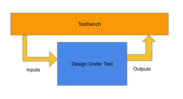
Figure 2: Testbench and the DUT
Testbench needs to work over a wide range of abstraction levels, creating sequences and transactions that are eventually translated into bit vectors. One of the main important features of the testbench should be maximum code reuse. To verify a complex ASICs with many features, we should write hundreds of directed tests. If constrained-random stimulus is used far fewer tests will be needed. The real work of the verification engineer is put into constructing a testbench that contains all the lower layers of the testbench: scenario, command, functional. The testbench code is used by all the tests which means it should be generic. To see how this architecture looks like, please check the system Verilog environment examples. There are different tools for HDL verification by EDA companies such as Synopsys, Mentor Graphics, Cadence. An example of a simple testbench for a ripple adder using Synopsys’s VCS is shown below:
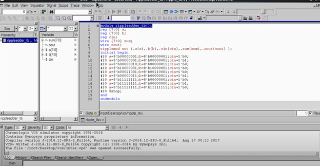
Figure 3: Ripple adder testbench using VCS
The input and output signals (waveform) using this testbench and DUT (ripple adder) which is instantiated in the testbench for applying input signals and checking the outputs on the same VCS environment is shown below:
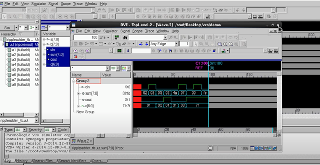
Figure 4: Input and output signals of ripple adder in VCS environment
One of the most important parameters of functional verification is functional coverage. We must run verification to make sure that the desired coverage is achieved. If all input and output combinations are checked we say that 100% functional coverage is achieved. Only in that case we can be sure that our design will work properly. After the synthesis of RTL and applying constraints (timing, area, power consumption), we should verify the design again. In this case both functional as timing verifications are performed. It is then followed by physical design and verification again. After physical design (layout, placement, routing) both functional and non-functional verifications should be done which will take into account physical models and parasitic capacities of the components. LVS (Layout versus schematic) and DRC (design rules check) are also applied. DRC makes sure that our design keeps the rules by the technology it is designed for so that manufacturing it will be possible. LVS makes sure that our layout and schematic are identical, basically we have built the layout of the design we wanted to. We run our simulations what we call for different PVT (process, voltage, temperature) corner cases. There are many cases of which three are the most important: TT, FF, SS. Typical or TT case is when we have our typical supply voltage, the manufacturing process went normal and temperature is 25 degree Celsius (room temperature). FF is the fast case when our supply voltage goes up +10%, our manufacturing process created faster components and the temperature is -40 degree Celsius (which makes transistors faster). SS is the slow case when our supply voltage drops for 10%, our manufacturing process hypothetically produces slower components and the IC should work for 125 degree Celsius. Checking all these three corner cases is important because we don’t know how the manufacturing process will go and we ensure that our IC will work from -40 to 125 degree Celsius. Also, the supply voltage may go up or down. SS case is especially critical for making sure we have no set up time valuations, while checking FF case is important for making sure we have no hold time violations.
While there are many things common when it comes to ASIC verification workflows and tools used regardless of IC type, there are also some differences. Since analog circuits are designed manually the tools and analysis used for them in some way differs from that of digital ASIC which is mostly using automated design. For the analog IC we don’t write HDL code, instead we use components to build them manually. Synopsys has a tool called Custom Designer that allows doing this. We create the schematic and then can use the same environment for creating testbench as well. A schematic of an Operational amplifier and its test on Synopsys Custom Designer environment using SAED (Synopsys Armenia Educational Department) library is shown below (Source: “The design and research of digital processing method for analog signals” – Roza Bejanyan, master thesis):
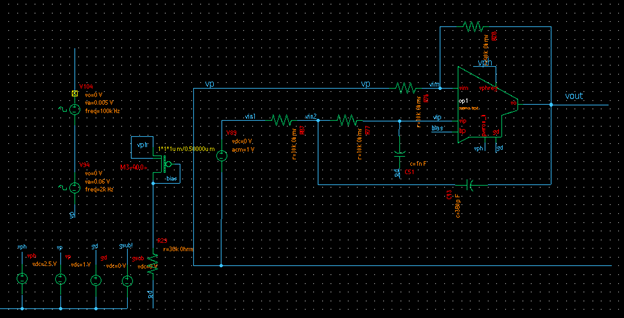
Figure 5 :Operation Amplifier under the test in Synopsys Cdesigner environment
From Cdesigner a Spice netlist is generated. We run spice simulations to make sure that the design is working. A simulation is also run after physical design of an analog IC. Similar Spice netlist is generated and verified after physical design for Digital integrated circuits. Running corner cases for TT, FF and SS applies for analog IC as well. The following simulations are part of a verification process for an Analog IC:
The AC analysis for the circuit shown in Figure 5 for TT, FF and SS cases using Hspice simulation is shown below:
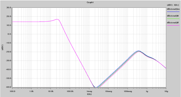
Figure 6: AC analysis for TT, FF, SS cases using Hspice simulation
Mixed signals IC is a circuit that has both analog and digital parts. Their verification process includes both analog and digital workflows and methods.
Get a fast indicative cost range, then unlock a full breakdown by email.
ASIC design is 80% about ASIC verification since the integrated circuits are becoming more complex and any failure is very costly. The cost increases exponentially with time and stage it is detected. There are some specific approaches for verification depending on the IC type, but they also have many things in common. Verification happens in parallel and in all stages of ASIC design. After manufacturing a post silicon validation is used.
