

The DFN (Dual Flat No-leads) and its counterpart, the QFN (Quad Flat No-leads), are increasingly prevalent in high-performance applications. They’re favored for applications ranging from consumer electronics to automotive systems due to their ability to support advanced circuitry in a small footprint. Familiarizing yourself with these packages’ specifications can dramatically improve design strategies and product efficiency.
This ultimate guide delves deep into the world of DFN packages, exploring their benefits over other packaging options and highlighting their key applications. Through a detailed analysis, we will cover everything from the importance of epoxy molding compounds to the steps for optimal DFN integration, providing insights and resources to harness DFN packages for modern electronics.
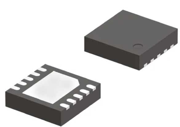
The Dual Flat No-Lead (DFN) package is a type of electrical package known for its compact design and efficient performance. As opposed to normal packages, DFN packages offer superior electrical and thermal performance. Their small package size and low-profile design are ideal for modern electronic devices.
Features of the DFN Package:
These flat no-lead packages, are also known as MLPQ (Micro-Leadframe Package Quad), are part of a versatile component package family. They cater to various versions with pads and suit a wide range of integrated circuit designs. DFN’s small package dimensions provide an efficient solution for designers aiming to minimize thermal expansion while maintaining robust electrical connections.
Dual Flat No-Lead (DFN) packages are types of chip scale packages used in electronic devices. Both offer excellent electrical performance and compact package size, making them ideal for modern gadgets. They are part of the flat no lead package family, known for their high thermal performance and low-cost implementation.
Key Features:
Both DFN and QFN packages support modern electronics by providing reliable electrical connections and reducing package dimensions. This makes them essential in integrated circuits. As a package designer, understanding these characteristics is crucial for selecting the right component package for various applications.
The Dual Flat No-Lead (DFN) package is a type of chip scale package that offers several advantages for electronic devices. Its small package size and excellent electrical and thermal performance make it ideal for many applications.
Key Applications:
DFN packages, with their versions with pads and metal pads, lead the category of packages favored for both general and specific applications in component package families.
The Dual Flat No-Lead (DFN) package is gaining popularity due to its numerous advantages over other packages.
Key Benefits:
DFN packages offer a blend of performance, cost-effectiveness, and reliability, making them a preferred choice for modern electronic designs.
The Dual Flat No-Lead (DFN) package is a type of chip scale package widely used in electronic devices. It excels in offering efficient electrical connections through its metallic pads. Unlike traditional leaded packages, the DFN package has no extended leads, which significantly reduces the package size and enhances thermal performance.
Key Features of DFN Packages:
DFN packages are part of the broader category of flat packages, known for low-cost and efficient designs. They resist moisture absorption, maintaining performance even in humid environments. Their pad counts and package dimensions are flexible, catering to various integrated circuits.
DFN packages offer an ideal balance of performance and compactness in modern electrical designs.
Reliability testing for Dual Flat No-Lead (DFN) packages is crucial to ensure durability and performance in electronic devices. These tests assess how DFN packages handle stress factors such as thermal expansion, moisture absorption, and electrical connections.
Key Aspects of DFN Reliability Testing:
DFN packages, known for their compact package size, must endure rigorous conditions. These conditions mimic real-world environments they encounter in various component package families. Reliable performance is vital to avoid failures in integrated circuits and mount plastic packages. Versions with pads and metal pads are particularly tested to verify pad counts and land pattern suitability.
Reliability tests ensure DFN packages meet the demands of modern electronics, providing confidence to Package Designers in the category of low-cost packages.
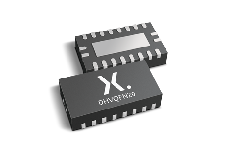
DFN Package vs. QFN: A Comparative Analysis
The Dual Flat No-Lead (DFN) Package and Quad Flat No-Lead (QFN) Package are popular component package families. Both are used for integrated circuits and electronic devices due to their compact package size. Here’s a quick comparison:
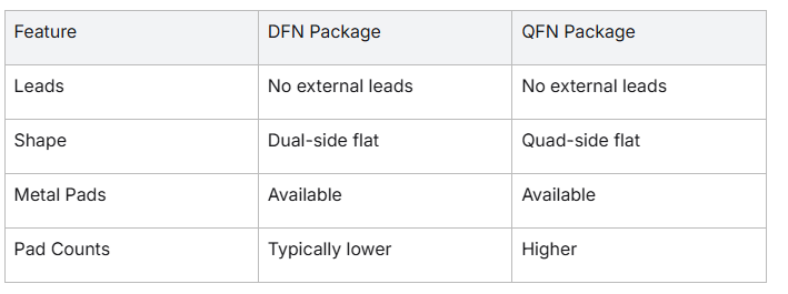
Key Differences:
Considerations for Designers:
In summary, choose DFN for simplicity and QFN for better performance.
Dual Flat No-Lead (DFN) packages are widely used in the electronics industry. They offer a compact package size and good thermal performance. These qualities make them ideal for many applications. DFN packages are often chosen for their simplicity and cost-effectiveness. Their metal pads allow for efficient electrical connections, enhancing overall device performance. Due to their small package size, DFNs fit well into compact electronic devices, like smartphones and tablets. Designers prefer DFNs for applications needing less complex electrical circuits. They are also effective in reducing moisture absorption, which improves device durability. In instances where a lower pad count is sufficient, DFNs provide an excellent option. Their versatility is why they are a staple in many electronic products today.
Bipolar transistors are a key component in DFN packages. They are used to amplify or switch electronic signals, playing a crucial role in a device’s operation. DFN packages house these transistors effectively due to their compact size and robust thermal performance. The metal pads on DFNs aid in managing heat, ensuring that bipolar transistors function efficiently. This is particularly important in preventing overheating, which can damage components. In addition, the layout of a DFN package supports better signal integrity. This enhances the transistor’s performance in the circuit. As a result, DFN packages are popular for applications requiring stable and reliable transistor operations. Whether in consumer electronics or industrial controls, DFNs deliver high performance without sacrificing space.
Diodes are integral to many electronic circuits, and DFN packages provide an ideal housing solution. The small package size of DFNs allows them to fit easily into compact designs. This is crucial for portable devices where space is at a premium. Metal pads in DFN packages enable efficient electrical connections for diodes, reducing energy loss. Diodes housed in DFN packages benefit from reduced thermal resistance, supporting their long-term reliability. This ensures that circuits operate smoothly without fluctuations in performance. DFN packages also offer protection against environmental factors like moisture, which can impede diode function. This packaging choice is perfect for applications where space and reliability are prioritized. Thus, DFN packages are a preferred option in mobile technology and automotive electronics.
MOSFETs, or Metal-Oxide-Semiconductor Field-Effect Transistors, are common in electronic circuits. DFN packages are an excellent choice for housing these components due to their efficient space utilization. The DFN’s compact size allows for integration in tight spaces, accommodating portable and small-scale electronics. The arrangement of DFN metal pads provides reliable electrical connections, crucial for MOSFET performance. Moreover, DFN packages offer superior thermal expansion capabilities. This ensures that MOSFETs operate within safe temperature ranges, reducing the risk of failure. DFNs also have low thermal resistance, which aids in heat dissipation, extending the lifespan of the MOSFETs. Therefore, DFN packages are favored in power management systems and high-frequency applications. They provide reliable MOSFET integration, enhancing circuit performance and durability.
Integrating a Dual Flat No-Lead (DFN) package into electronic devices involves several key steps to ensure optimal performance.
Each step ensures your DFN package functions optimally, providing a flat no-lead solution with excellent performance.
DFN (Dual Flat No-Lead) packages are popular in electronic devices due to their excellent electrical and thermal performance. They offer efficient electrical connections and support compact design, important for integrated circuits. Knowing the right resources can help in optimizing the use of DFN packages.
Key Resources:
Using these resources ensures effective use of DFN packages, enhancing the design and performance of component package families in various applications. For custom or advanced applications, engineers often look into versions with pads tailored to their specific needs.
Dual Flat No-Lead (DFN) packages are gaining popularity in electronics. Their small size and low cost make them ideal for integrated circuits. As technology advances, the future looks promising for DFN packaging.
Key Trends:
These trends indicate DFN packages will continue to evolve, meeting the needs of modern electronic devices. Whether for consumer electronics or industrial applications, DFN technology remains a key component in the future of integrated circuits.
For electronic devices, DFN packages present a step forward in package design. Whether for mounting in low-profile applications or dealing with thermal management, the dual flat no-lead package sets the standard for efficiency and reliability in modern component package families.
Get an indicative packaging cost range, then a detailed breakdown by email.
