

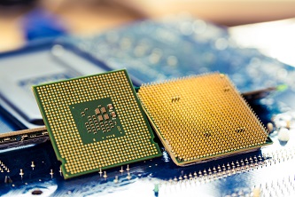
Figure 1 – Example of Integrated Circuit
An integrated circuit is defined as a set of electronic circuits on one small flat piece of semiconductor material, most frequently silicon. It is also referred to as an IC, a chip, or an ASIC.
Onto a small chip a large number of tiny MOSFETs (Metal-Oxide-Semiconductor Field-Effect Transistors) are placed and interconnected to create an IC. This results in circuits that are orders of magnitude faster, smaller, and less expensive than their discrete counterparts, which are constructed using discrete electronic components.
Due to the mass production capability, reliability, and the building-block approach to integrated circuit design, the electronics industry has rushed to adopt standardized ICs in place of designs using discrete transistors, with ICs having two main advantages over discrete circuits: performance and cost.
Performance is considerably higher in ICs than their discrete counterparts because the components inside an IC have shorter switch times and consume a lot less power due to their small size and proximity to each other.
When it comes to cost, it is very low because ICs are printed as a unit using photolithography, instead of being constructed one transistor at a time. As an added benefit, packaged circuits use much less material than similar discrete ones.
ICs do have a big disadvantage, though: the high costs involved in designing them and in fabricating the photolithography masks. Due to this, ICs are commercially viable only when high production volumes are anticipated, so that the profit margins can justify them.
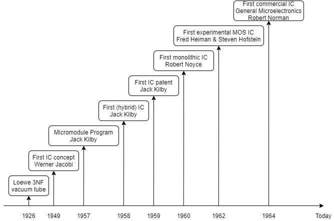
Figure 2 – History Timeline of ICs
Metal-Oxide-Silicon (MOS) semiconductor device fabrication and all the associated technological advancements made ICs more and more practical. Since their beginning in the 1960s, the capacity, speed, and the dimensions of ICs have vastly increased, driven by technical advances that fit more and more MOS transistors on chips of the same size.
The Loewe 3NF vacuum tube from the 1920s was the earliest attempt at combining several components into one device (the idea behind modern ICs), but, unlike ICs, it was designed with the purpose of tax avoidance. In Germany, radio receivers had a tax that was correlated with the number of tube holders a radio receiver had, so this first attempt allowed radio receivers to have a single tube holder, while not sacrificing functionality.
The first concepts of a real integrated circuit go back to 1949, when German engineer Werner Jacobi (Siemens AG) filed a patent for an integrated-circuit-like semiconductor amplifying device, with the recommended industrial application of his patent being manufacturing and selling small and cheap hearing aids. Despite this, no immediate commercial use of his patent was observed.
One of the other proto-IC ideas was to create small ceramic substrates or micromodules which could be organized into grids of various complexities. Jack Kilby was the proponent of this idea in 1957. He pitched it to the US Army and that led to the short-lived Micromodule Program, but, as the project was getting started, Kilby came up with a new design.
Kilby had his initial thoughts about the integrated circuit in July of 1958, while working at Texas Instruments. He successfully showcased the first working example of a chip on the 12th of September, 1958. In his patent application from the 6th of February, 1959, Jack Kilby characterized his new device as “a body of semiconductor material … wherein all the components of the electronic circuit are completely integrated”. He eventually won the Nobel Prize for physics in 2000 for his part in the invention of the IC.
Kilby’s invention was not a precursor to current ICs, as it was a hybrid integrated circuit (hybrid IC), rather than a monolithic integrated circuit (monolithic IC) chip, because it had external wire connections, which made it very difficult to mass-produce.
So, Robert Noyce at Fairchild Semiconductor invented the first true monolithic IC chip half a year later. It was a new variety of microchip, more practical than Kilby’s, with Noyce’s design being made out of silicon, whereas Kilby’s chip used germanium. This monolithic IC put all components on a chip of silicon and connected them via copper lines. Thanks to these and many other reasons, modern IC chips are based on Noyce’s monolithic IC design, rather than Kilby’s idea.
The earliest experimental MOS IC was a 16-transistor chip built by Fred Heiman and Steven Hofstein, made at RCA in 1962. Following that, General Microelectronics introduced the first commercial MOS IC in 1964, which was a 120-transistor shift register designed by Robert Norman.
Today, as it becomes more and more difficult to manufacture smaller transistors, companies are using a multitude of techniques to increase performance and reduce size, without having to reduce the size of the transistors. Such techniques are collectively known as advanced packaging and include, but are not limited to: package on package, multi-chip module, three-dimensional ICs, high bandwidth memory and through-silicon vias utilizing die stacking.
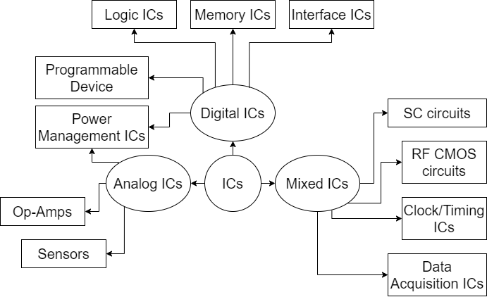
Figure 3 – Types of ICs
Integrated circuits can be classified into analog, digital and mixed signal circuits.
Digital chips can contain billions of logic gates, multiplexers, flip-flops, and other smaller circuits in a few square millimeters. This small size allows the circuits to have high speed, low power dissipation, and reduced manufacturing cost. At the core of digital ICs is boolean algebra, used to process the 0 and 1 signals.
Some of the most advanced and well-known digital ICs are the microprocessors (also known as CPU), which are used in PCs, smartphones, smart appliances etc., followed by digital memory chips and other application-specific integrated circuits (ASICs).
Digital ICs can be further categorized as:
Analog ICs are different because they process continuous signals and perform analog functions such as amplification, demodulation, mixing, and active filtering. Some notable examples of analog ICs are: sensors, power management circuits, and operational amplifiers.
There are also ICs that can combine analog and digital circuits on a chip to create special functions such as analog-to-digital converters and digital-to-analog converters. These mixed-signal circuits offer smaller size and lower cost but must take into account signal interference (due to the use of analog components and signals).
Mixed-signal ICs can be categorized as follows:
IC design flow can be divided in two broad categories: digital and analog.
Digital IC design refers to the process behind the production of components such as microprocessors, memories (ROM, RAM, and flash), FPGAs, and digital ASICs, focusing on maximizing circuit density, logical correctness, and placing circuits in such a manner that clock and timing signals are routed properly.
On the other hand, analog IC design specializes in power IC design and RF IC design, being used in op-amps, phase locked loops, linear regulators, oscillators and active filters. Analog design is more concentrated on the underlying physics such as gain, power dissipation, matching, and resistance. The fidelity of analog signal amplification and filtering is also critical, so analog ICs have to use a larger active area than digital designs and are usually less dense in circuitry.
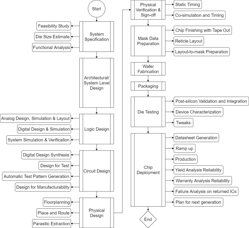
Figure 4 – IC Design Steps
A typical IC design cycle involves several steps:
System Specification
Logic Design
Circuit Design
Physical Design
Physical Verification & Sign-off
Mask data preparation (Layout Post Processing)
Wafer fabrication
Packaging
Die test
Chip Deployment
For digital IC design in particular, the process can be divided into three parts: ESL, RTL and Physical Design.
To be noted that RTL (also called front-end) is responsible for the chip functionality, while the physical design (also called back-end) is more focused on the chip layout.
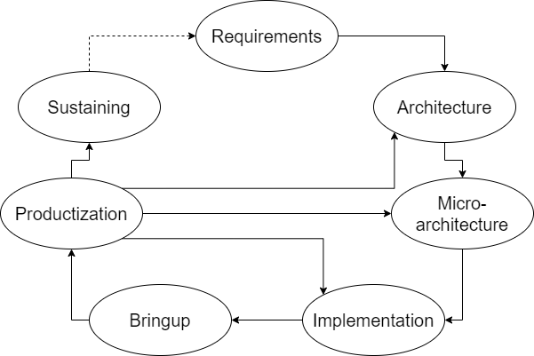
Figure 5 – IC Design Lifecycle
The integrated circuit (IC) development process starts with defining product requirements, progresses through architectural definition, implementation, bring up and finally production. The various phases of the integrated circuit development process are shown in Figure 5. Although the phases are sometimes presented in a straightforward fashion, in reality there is iteration and these steps may occur multiple times.


