

Static Timing Analysis is defined as: a timing verification that ensures whether the various circuit timing are meeting the various timing requirements.
One of the most important and challenging aspect in the ASIC/FPGA design flow is timing closure. Timing closure can be viewed as timing verification of the digital circuit. A digital circuit which is closed for timing will work at specified frequency (defined by designer in timing constraints) and thus promised PPA (performance, power and area) can be achieved. Static timing Analysis is the method by which one can determine if timing closure is achieved or not by doing timing analysis on all paths within the digital circuit. As the name suggest this kind of verification of digital circuit is done statically (no simulation of the digital logic is required). Static timing analysis make use of the timing arcs (defined by technology library) between all the start and end points of the digital circuit. One must be aware that since there is no simulation involved, static timing analysis will not check for functional correctness, rather it will only focus on timing.
Before we dig deeper into how static timing analysis works, it is valuable to get some basic knowledge of terms used later.
Timing Arcs: The timing arcs are parameters defined in the process library for each cell which define the delays of the cell across different PVT corners. static timing analysis uses those parameters to calculate the max and min delay through any library cell. For example, for a D Flipflop, technology library will include the parameters that define the setup time, hold time and C (clock) to Q (output) time (TCQ).
TCQ: The TCQ is defined as time it takes for data to appear on output Q once clock C is triggered (pos edge or neg edge)
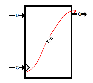
Figure 1: D – Flip Flop TCQ Timing Arc
Setup time: The time the input D must be stable before the clock C is triggered (pos edge or neg edge) is defined as setup time. If the data is not stable at least setup time before the clock edge, output will be undetermined.
Hold time: The time the input D must be stable after the clock C is triggered (pos edge or neg edge). If the data is not stable for at least hold time after the clock edge, output will be undetermined.
Static timing analysis can be done on both sequential and combinatorial parts of the design. In any sequential design path there is always one launch flop (driving the data) and one latch flop (capturing the data). Combinational paths can also be considered as sequential paths by assuming a virtual clock driving a virtual launch or virtual latch flop.
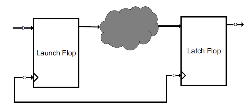
Figure 2: Sequential path
Setup constraint: The setup constraint of any digital circuit is defined as the timing constraint so that the slowest path in the design must meet setup time of the latch flip flop.
Hold constraint: The hold constraint of any digital circuit is defined as the timing constraint so that the fastest path in the design must meet hold time of the latch flip flop.
If a design fulfills both setup and hold constraints, the design is said to have achieved timing closure. static timing analysis will prove/disprove the setup and hold constraints by analyzing all the timing paths in the design.
Any digital design can be divided into four categories of paths for static timing analysis.
Static timing analysis is done on all these paths one by one. Each path is analyzed separately by defining the start and end points in that path. Let us first consider static timing analysis for the R2R paths. They are simple and become basis for other paths.
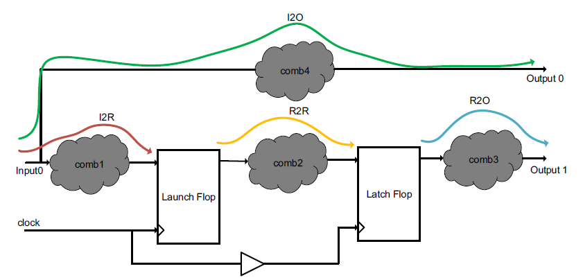
Figure 3: Design Example for static timing analysis
For R2R paths, the start point is clock input pin of the launch Flip Flop and end point is D input pin of the latch flop. For setup constraints, the goal is to make sure that delay from start point to end point is at least setup time of latch flop less than clock period of the latch clock. This means that
TCQ + comb_delay(max) < clock delay path (clock skew) + T (clock period of clock) – setup time of latch FF
comb_delay in below figure should be maximum delay through the combinatorial cloud.
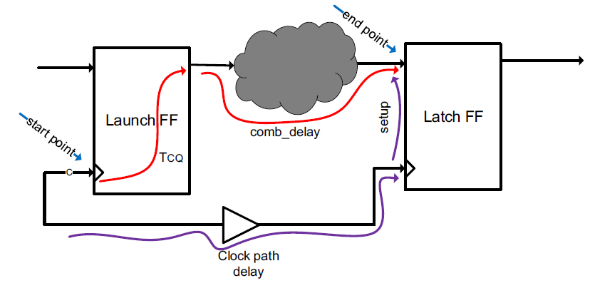
Figure 4: Setup constraint for R2R paths
For hold constraint, the goal is to make sure that delay through start and end point is at least more than the hold time of the latch flop in same clock cycle.
TCQ + comb_delay (min) > hold time of latch FF + clock delay path (clock skew).
comb_delay in below figure should be minimum delay through the combinatorial cloud. One can observe that hold time do not depend on the clocking period of the clock.
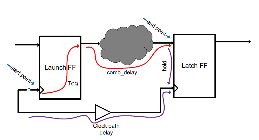
Figure 5: Hold constraint for R2R paths
For I2R paths, the start point will be input ports and an end point will be D pin of the latch flop. One can assume an input delay from the input port to the combinatorial cloud as show below. The input delay can include pad delay or any net delay.
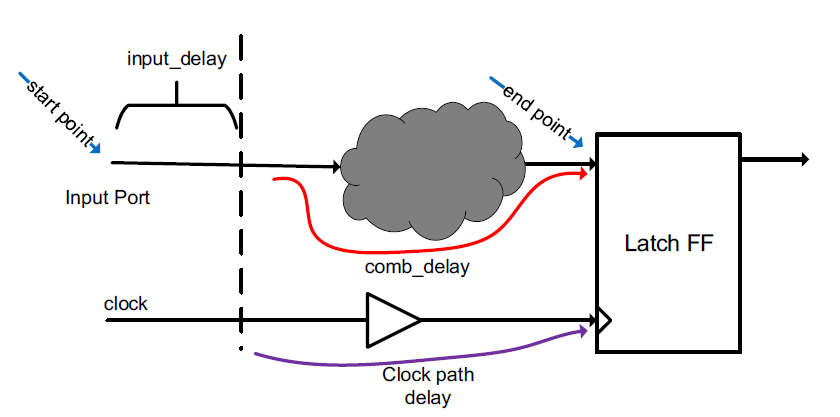
Figure 6: Setup/hold constraints for I2R paths
If the input ports are synchronous to external clock, the paths can be constrained for setup as,
input_delay + comb_delay (max) < clock delay path (clock skew) + T (clock period of clock) – setup time of latch FF
And For the hold constraints as
input_delay + comb_delay (min) > hold time of latch FF + clock delay path (clock skew).
If input is not synchronous to clock, the path can be constrained with max and min delay for the path from input port to D pin of the Latch FF. Normally in such cases (a synchronous path latched by clock) requires two latching FFs back to back to remove metastability issues.
input_delay + comb_delay(max) < max_delay (required)
input_delay +comb_delay (min) > min_delay (required)
For R2O paths, the start point will be clock pin of the launch flop and an end point will be output port. One can assume an output delay from the output of combinatorial cloud as show below. Output delay can include pad delay or the net delay from combinatorial cloud to pad.

Figure 7: Setup/hold constraints for R2O paths
If the output ports are synchronous to the clock, the paths can be constrained for setup as,
TCQ + comb_delay (max) + output_delay < clock delay path (clock skew) + T (clock period of clock) – setup time of latch FF
And For the hold constraints as
TCQ + comb_delay (min) > hold time of latch FF + clock delay path (clock skew).
If the output path is not synchronous to clock, the data path can be constrained with min and max delays.
TCQ + comb_delay(max) + output_delay < max_delay (required)
TCQ + comb_delay (min) + output_delay > min_delay (required)
For I2O paths, the start point is input port whereas end points are output ports. One can assume input delay for input ports and output delay for output ports. Normally the combinatorial paths between inputs and output ports are constrained so that minimum and maximum delay constraints are met.
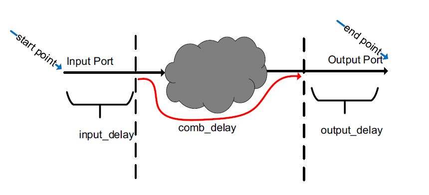
Figure 8: Min/Max delay constraints for I2O paths
input_delay + comb_delay (max) + output_delay < max_delay (required)
input_delay + comb_delay (min) + output_delay > min_delay (required)
One can also assume that a virtual launch Flip Flop driving the input port and virtual latch flop latching the output port. In such scenario, the analysis can be done just like R2R paths.
Static Timing Analysis Tips & Tricks


