

In semiconductor design, “sign-off” during the tape-out (tapeout) of a chip refers to the formal approval process to ensure that the chip design is error-free, meets all specifications, and is ready for manufacturing at the foundry. It is essential because it minimizes the risk of costly errors, ensures compliance with foundry requirements, and validates that the chip design is production-ready before fabrication begins. Sign-off is a critical quality control checkpoint in the chip manufacturing process. Download our tapeout checklist here.
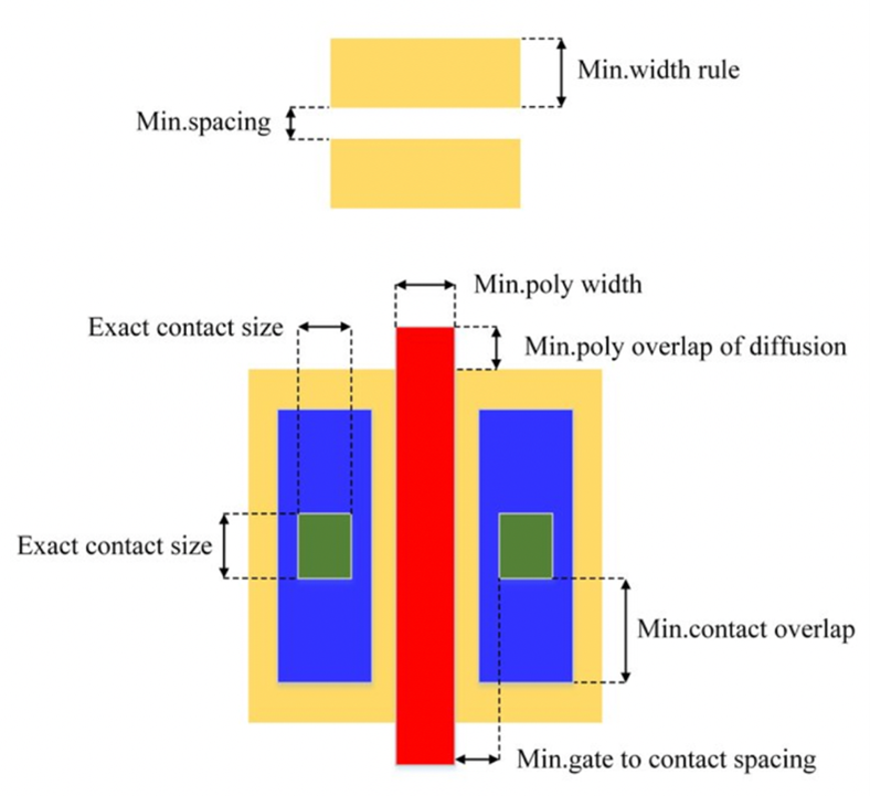
Design Rule Checks are automated checks performed on the layout of a semiconductor chip to ensure that the design adheres to the specific design rules and constraints provided by the semiconductor foundry or manufacturing process. These design rules encompass various factors such as minimum feature sizes, spacing, layer alignments, and other manufacturing constraints. DRCs help verify that the chip design is manufacturable using the chosen semiconductor process technology. They ensure that the design adheres to the physical limitations and capabilities of the manufacturing process. Failure to perform adequate DRC checks can lead to manufacturing failures, increased production cost, reduced chip yield, delayed product development, and compliance issues. Examples of some common DRCs:
Minimum Feature Size: Ensures that the smallest geometrical features (metal lines, vias, transistor gates etc.) meet or exceed the minimum allowable size specified by the semiconductor process technology.
Spacing Rules: Checks that there is sufficient space between adjacent features, preventing short circuits or other electrical issues. This includes checks for minimum spacing between metal lines, vias, and other elements.
Width and Length Checks: Verifies that various elements, such as transistor channel widths or wire lengths meet specified dimensional requirements.
Dummy Fill Rules: Checks that dummy fill insertion, which helps ensure planarity and manufacturability, follows prescribed guidelines.
Antenna Rules: Verifies that appropriate measures are taken to prevent charge buildup and potential damage during programming or erasing of non-volatile memory cells.
Tool like Mentor Graphics’ Calibre, Synopsys IC Validator are used for verification of design DRCs.
Timing analysis is a crucial sign-off activity to ensure that the design meets the frequency specification as advertised. It comprises of two main buckets:
Validating the timing constraints: Timing constraints are a set of rules and parameters defined in digital design to capture the functional intent of the design in terms of clock definitions, and their frequencies across various functional and test modes. They also capture other conditions like false paths, multi-cycle paths which ensure that the timing constraints are not pessimistic which may impact power and area.
Timing Closure: Timing closure is the process of iteratively refining a digital design to meet its timing constraints. It involves multiple steps including synthesis, placement, routing and optimization to ensure that the design operates correctly at the specified clock frequency. In addition to meeting the setup time and hold time constraints, it also ensures that there are no transition violations, maximum capacitance violations, glitch violations in the design.
Perhaps the biggest challenge with timing closure lies in meeting the performance targets while avoiding lengthy design iterations. Designers use timing analysis tools like Synopsys’ PrimeTime, Cadence’s Tempus or Mentor Graphics’ xACT to check for setup and hold timing violations, clock domain crossings and overall performance.
Power analysis quantifies the power dissipation of the design under various operating conditions and across myriad functional scenarios. It is a critical sign-off activity to ensure that the chip operates within specified power constraints. It is important not only from a standpoint of power efficiency where higher power efficiency translates into higher battery life, but also from a standpoint of thermal management. Higher power consumption generates heat, which can degrade chip performance, reduce reliability, and even cause thermal failures.
Power analysis is performed at early stages to estimate power consumption and verify it doesn’t exceed design limits. It involves identification of design hierarchies consuming most power, and if the numbers are more than the specification, designers pro-actively work to identify ungated registers in the design and try and move them to the gated clock, if possible. In other cases, designers may choose to implement fine grained clock gating to bring the power dissipation under check for most common use-cases. Power gating, on the other hand, has architectural implications, and can be very useful in reducing the leakage power of the design. The major challenge with power optimization lies in balancing it with performance requirements. Designers use tools like Synopsys’ PrimePower and Synopsys’ PTPX for power analysis.
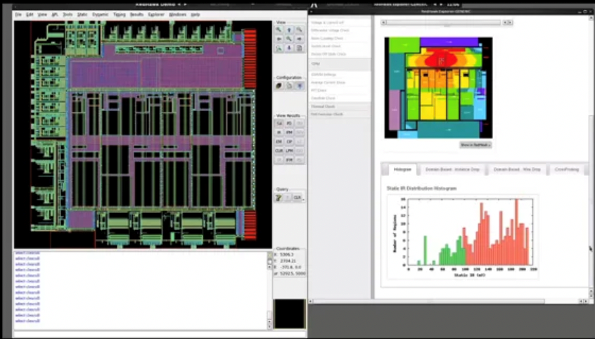
Power integrity checks, including dynamic and static IR drop analysis, are essential steps in the verification process of electronic designs. These checks help ensure that the distribution of electrical power within a circuit or system meets specified requirements and avoids issues related to voltage drop, noise and reliability.
Static IR Drop Analysis: Static IR drop analysis focuses on assessing the voltage drop across the power distribution network under steady state or DC (direct current) conditions. It aims to identify voltage discrepancies and ensure that all components in the design receive the required supply voltage. If the voltage drops are excessive, it can lead to functional failures, timing violations, and decreased overall performance of the electronic system.
Dynamic IR Drop Analysis: Dynamic IR drop analysis assesses the transient or AC voltage variations in the power distribution network during the switching of digital logic gates or other dynamic events in the design. Excessive dynamic IR drop can lead to data errors, timing violations, and electromagnetic interference (EMI) issues. It helps design engineers assess the impact of dynamic current demands on the power distribution network and implement mitigation strategies like proper decoupling capacitors and power grid design.
Electromigration: Electromigration refers to the gradual displacement of atoms in the metal wires due to the movement of ions within the metallic interconnects induced by the flow of electric current. It can cause shorts or open in the metal interconnects.
Most commonly used EDA tools for power integrity analysis are ANSYS’ Redhawk, ANSYS’ Redhawk-SC and Cadence’s Voltus.
Electrical Rule Checks (ERCs) are a set of automated checks performed during the electronic design verification process to ensure that a circuit design adheres to specific electrical connectivity and functionality rules. These checks are essential for identifying and preventing electrical errors and issues that could lead to functional failures or safety hazards in electronic systems. Common types of ERCs are as follows:
Connectivity Checks:
Short Circuit Checks:
Open Circuit Checks:
Mentor Graphics Calibre, Cadence Virtuoso, Synopsys Fusion Compiler, ANSYS Slwave are some of the EDA tools proficient with detecting ERC violations.
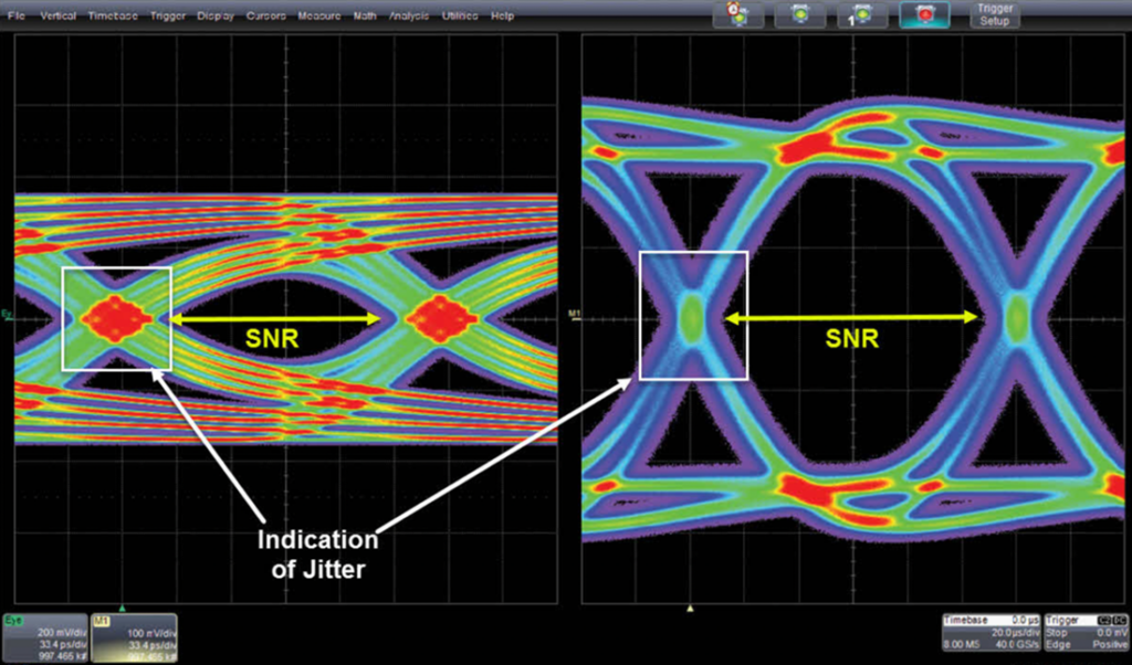
Signal Integrity Analysis is the process of evaluating and optimizing the quality and reliability of electrical signals as they propagate through electronic components, interconnects, and printed circuit boards (PCBs). The goal is to ensure that signals remain intact and free from distortion or noise. One key aspect of signal integrity analysis is to analyze and minimize signal reflections, and to account for transmission line characteristics such as impedance matching and termination that can distort waveforms and lead to signal integrity issues.
SPICE simulators like Cadence Spectre, Synopsys HSPICE along with Cadence Sigrity are used for signal integrity analysis.
Electromagnetic interference analysis is the process of assessing and mitigating the electromagnetic emissions and susceptibility of electronic devices and systems to prevent the unintentional generation of electromagnetic interference that can disrupt other devices or systems.
Ansys EMIT and Keysight EMPro are some of the EDA tools used for EMI analysis.
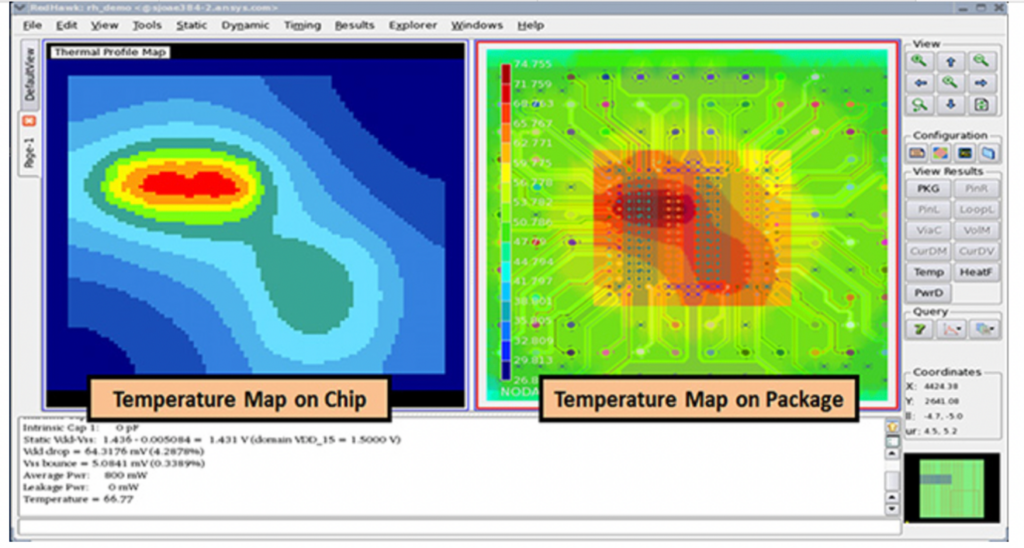
Thermal analysis assesses the thermal behavior of the chip to prevent overheating and to ensure reliability. It checks the following:
Temperature Distribution: Evaluate temperature distribution across the chip under different operating conditions and scenarios. The temperature distribution also guides the designers regarding the optimal locations to place the temperature sensors if they are supported by the architecture. These temperature sensors can cause the frequency or the voltage to scale down to prevent overheating.
Thermal Management: Verifies the effectiveness of thermal management techniques such as heat sinks or thermal vias.
Hotspot Detection: Detects the local hotspots and can motivate floorplan changes to address them.
Thermal analysis tools rely on computational fluid dynamics (CFD) software and thermal simulation tools. ANSYS IcePack, Mentor Graphics FloTherm are some of the tools used in thermal analysis.
Electrostatic discharge refers to the sudden and momentary flow of electricity between two objects at different electric potentials. In semiconductor manufacturing and handling, ESD is a significant concern because it can potentially damage or destroy sensitive electronic components and integrated circuits (ICs). ESD verification confirms that the chip is protected against ESD events. Designers use ESD clamps that offer a low resistance path for the electricity to flow, thereby bypassing the electrical circuitry. Foundries often recommend a distance or a resistance based spec to be met to ensure the number and the clamps are sufficient and well distributed to prevent an ESD event from damaging the internal circuitry.
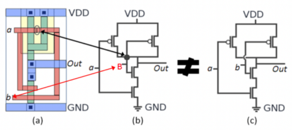
Layout versus Schematic (LVS) is an automated process that checks whether the physical layout of a semiconductor design matches its intended schematic or logical representation, It ensures that the actual physical layout accurately reflects the designer’s intended circuit functionality. LVS involves:
Creating a schematic: During initial design phase, engineers create a logical or schematic representation of the integrated circuit, This schematic defines the components, their connections, and their electrical characteristics.
Creating the layout: After creating the schematic, engineers proceed to create the physical layout of the circuit, specifying the position, size, and connectivity of each component on the semiconductor chip.
LVS Verification: The LVS tool compares the physical layout (GDSII file format) with the original schematic (in the netlist format). It checks for consistency in terms of connectivity, component placement, and electrical characteristics.
Tool like Mentor Graphics’ Calibre, Synopsys IC Validator are used for LVS verification.
Functional Verification
Functional verification ensures that the semiconductor device performs its intended functions correctly and accurately. It aims to detect and rectify design errors, bugs and functional issues before manufacturing or deployment. Some key aspects of functional verification are:
Simulation: Simulation is the primary technique used for functional verification. It involves running the design through simulation software to simulate various input conditions and verify that the outputs match the expected behavior. Simulation tools include: Cadence XSIM, Synopsys VCS and Mentor Graphics ModelSim.
Testbenches: Testbenches are sets of stimuli and test vectors used to drive the simulation. They provide the necessary input conditions to assess the design’s response and functionality.
Coverage Analysis: Coverage analysis tracks which parts of the design have been exercised during simulation. It helps ensure that the verification process is comprehensive and that all aspects of the design have been thoroughly tested.
Formal Verification: Formal verification techniques use mathematical methods to formally prove the correctness of a design. Formal Verification tools include Synopsys Formality and Cadence Conformal.
To conclude, the sign-off checks are the linchpin of semiconductor tape-outs, safeguarding the semiconductor industry’s ability to deliver advanced and reliable microchips. By rigorously validating the design against a multitude of criteria, these checks ensure that the ICs function correctly, adhere to manufacturing standards, and perform optimally.
Download our tapeout checklist here.
