

3D Through Silicon Vias (TSV) is in MEMS, CMOS Image Sensors and high-end applications. When will it be used for mainstream consumer applications?… All results are part of the new report released by Yole Développement (Yole): 3DIC & 2.5D TSV Interconnect for Advanced Packaging – 2014 Business Update. This technology & market report is an overview of the TSV implementation for various devices and packages including memories, logic, MEMS, photonics, CIS and other applications. The company analyzes future 3D products for high-end applications and alternative packaging technologies (fan-out, advanced organic substrates, monolithic 3D). Yole also details the market adoption roadmap and wafer start by platform and by application.
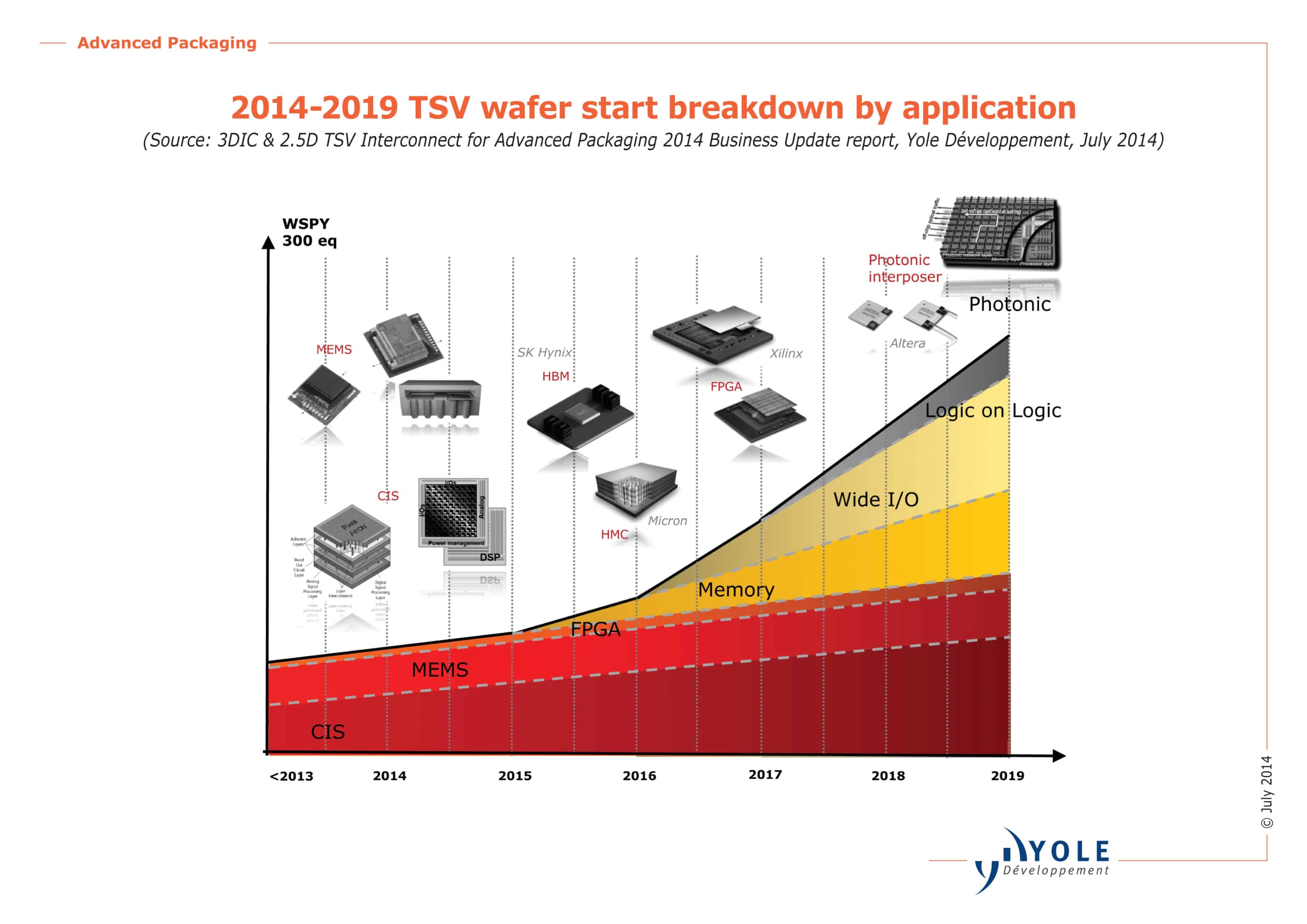
Through Silicon Vias (TSV) technology was adopted in production a few years ago for MEMS and CMOS Image Sensors (CIS).” Driven by consumer applications such as smartphones and tablets, this market is expected to continue to grow over the next several years. For high end memories, 2015 will be the turning point for 3D adoption”, explains Thibault Buisson, Technology & Market Analyst, Advanced Packaging at Yole. “Standards have now been established, therefore the industry will be ready to enter in high-volume manufacturing. Wide I/Os and logic-on-logic will follow, most probably around 2016-2017”, he adds. Emerging applications, such as photonics based on interposer, are also being developed for future products. However, their market entrance is most likely not going to happen before 2019-2020.
According to Yole Développement, market drivers have not changed over the years, fundamentally. Today, 3DIC is still driven by the need to increase performance and functionality, and to reduce form factor and cost. Adoption of 3DIC technology–due to its many advantages, as well as its ability to enable heterogeneous integration—is being considered for a wide range of applications.
“There is a significant advantage to using 3DIC and that is why this packaging platform is part of all the roadmaps of the key semiconductor players across the entire supply chain”, details Rozalia Beica, CTO & Business Unit Director, Advanced Packaging and Semiconductor Manufacturing.
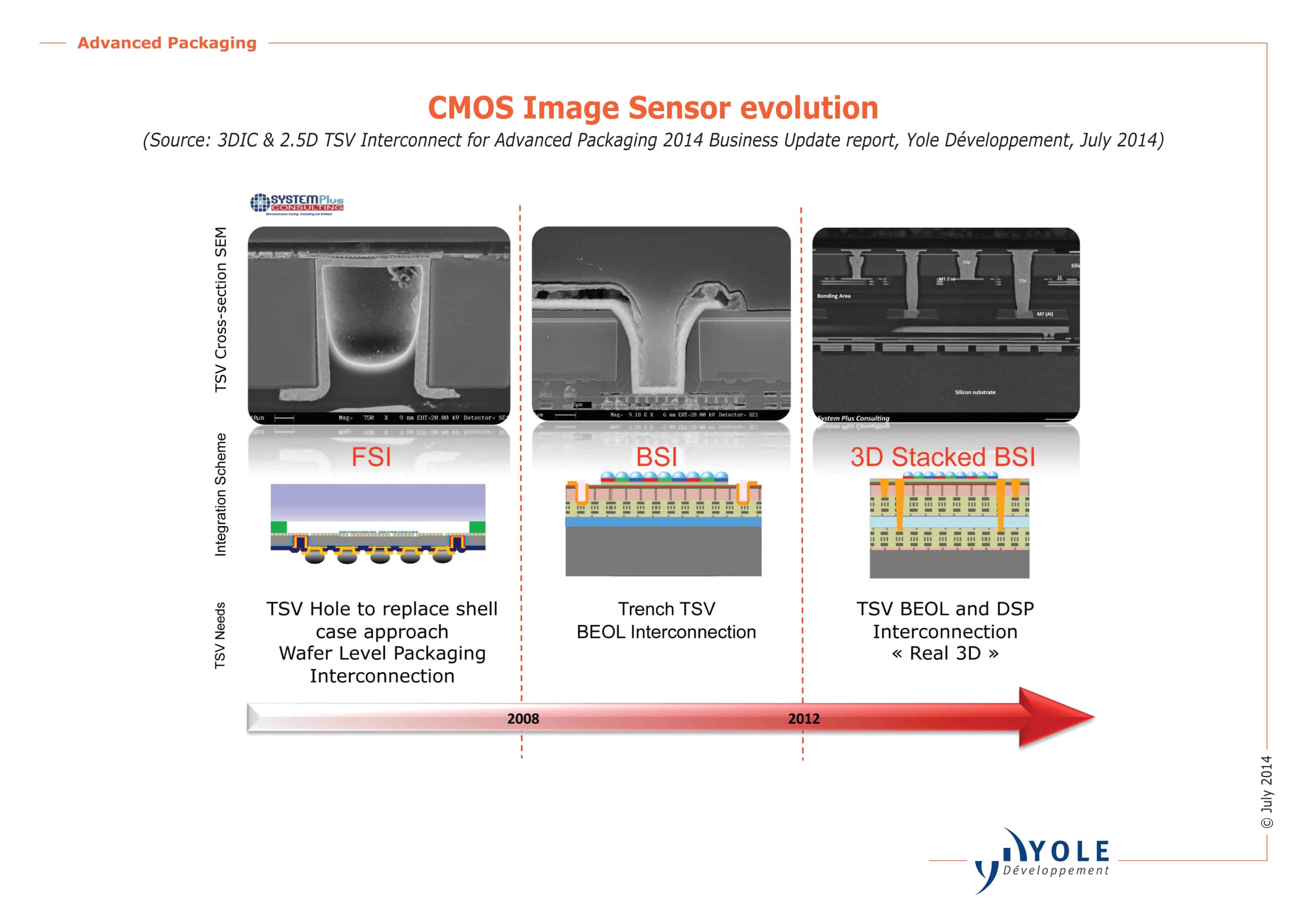
Once 3D is adopted it will never be dropped! In the CMOS Image Sensor application the evolution of TSV has never stopped. Even though the integration methods used for CMOS Image Sensors have changed and evolved over the years, TSV continued to be incorporated in the packaging of these devices, increasing functionality and enabling more efficient utilization of its silicon space. Sony, leader of the CMOS Image Sensor, by using a full-filled TSV and via last approach to stack the CIS onto a CMOS die, was able to more efficiently utilize (90%) of its die surface area for the pixel array while decreasing the size of the die. This technology, called Exmor, is using a 3D stacked integration approach, and, currently is the new trend for this type of devices as it enables a smaller die size and faster on-chip processing. The path is open for the heterogeneous integration of devices: MEMS are being integrated onto ASIC dies connected with TSVs (such as mCube, Bosch, with their accelerometer products, and others), and 3D stacked devices with integrated passives for medical applications, etc.
—————————————————————————————————————
This is a guest post by Yole Développement. Click here to read more from Yole Développement.


