

A recent on-line Blog by John Dunn (analog guru and prolific blogger) titled “The Weed-eater Circuit” got me thinking. Basically, John shared a simple 2 transistor schematic (Figure 1 shown below) that he has used as a test when he needed a way to see just how competent someone was at analog circuit analysis, somebody with whom he would soon be working. It sounds obvious to me. I had to pass a competency test to gain the privilege of driving a car. I had to pass several competency tests to get an engineering degree and the same for my ham radio license. You might even have a test for new engineering hires in your company.
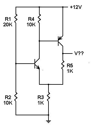
John does this because he understands exactly how complex and difficult analog design is; some say it’s far more so than digital design. John knows the pitfalls and wants to avoid them at all costs, including being very picky about who he works with.
I wish OEMs that engage ASIC companies in Analog or Mixed Signal developments would make note of this. Whether the requirement is a massive analog undertaking or only a small portion of the total chip, inexperience…okay, let’s be blunt… incompetence… in the ways of analog design is the single largest reason for failure in these designs.
In my 45 year analog career I must have heard over one-hundred horror stories about failed attempts to develop analog ICs. Let’s be brutally honest; it happens. Even big analog IC companies developing standard products sometimes have problems but they can afford to absorb the occasional failed attempts. They can either delay introduction until the chip works properly (as is often the case) or they can kill the part and move on to something else and no one is the wiser. To the outside world they have a perfect track record.
However, when an Analog ASIC chip bombs, those choices are not options. There’s a customer waiting, expecting that part to be ready for production. His product is nearly ready to go to market. He has a window of opportunity. The revenue he will derive from it depends on the ASIC being available on time and functioning to the agreed specification. There’s no room for error.
Unfortunately, the semiconductor industry has its share of analog pretenders; companies who claim false skills and experience in analog design; companies who will say just about anything to gain your confidence and win your order. The really sad part is that often they don’t realize that their claims are false because they “don’t know what they don’t know”. Caveat Emptor.
Analog behavior is described by sets of mathematical equations; digital is described by Boolean relationships. There is a distinct difference in the knowledge and skills required to fully understand and be competent in analog design. Analog ASIC designers need to know in depth about semiconductor manufacturing technology, semiconductor material chemistry and physics, semiconductor device physics, electrical circuit theory, control and feedback, thermodynamics and much more, while digital circuit designers need to know about Boolean algebra, linear algebra, digital signal processing, synchronous and asynchronous systems, timing delays, etc.. I’m not trying to imply digital design is easy… it’s not… but it is different… very, very different.
Stories I’ve heard recently about Analog ASIC development failures are beyond horror… they’re devastating. Customers calling and begging for help because the company they chose to develop their ASIC is having a problem. Initial samples are being tested and there are problems with the analog portion. Nobody knows what’s wrong. Worse yet, it seems no one knows how to fix them because the design team is often schooled in digital and has relied upon an analog cell library that was designed by a third party and they cannot possibly understand the intricacies of its behavior in relation to the chemistry and physics of the silicon process.
To compound the problem there are often three entities involved in creating your analog ASIC, all of whom are denying culpability; the company that designed the cell library of basic standard analog functions, the IC design company that used the analog cells in the chip design and the wafer fab that produced the silicon. Each one claims their part of the deal works fine. The problem must be one of the other guys.
Sadly, it’s an all too common situation. In today’s fast paced world, there’s no time for finger pointing. Customers seeking to develop an Analog ASIC need to understand that compared to digital circuits, designing Analog ASIC semiconductors requires more computational involvement and far greater knowledge of the actual semiconductor fabrication process to assure that every element in the design is rock solid.
It’s more than simply cobbling together some transistors to make an amplifier or A/D converter or picking certain functional blocks from a cell library and dropping them into a design. It requires deep intimate knowledge of the semiconductor process upon which the chip will be produced, and an understanding of the possible interaction of these. These are skills that are not necessarily required by digital designers. A note on a web site claiming analog or mixed signal design skills is no guarantee that what’s inside is actually a complete skill set to get it right.
Hence, John’s blog should serve as a wakeup call to those seeking to have an Analog ASIC developed. Before you retain the services of Analog ASIC semiconductor company, do your homework. Get to know the manager or team leader that will be assigned to your project. Don’t be shy. Verify his/her analog capabilities as well as the skills of the rest of the team.
I read a website comment recently; the source will remain nameless to avoid embarrassment. “Our vision is to put analog knowledge into the hands of a larger population of engineers with an electronics background, thereby making that pool of resources more substantial and impactful. Second, by putting a ton of analog knowledge into a software-defined platform, it frees up those critical Analog Engineers for high-value activities such as the very complex integration work that is often required.”
Implications of this bizarre statement are mind shattering. You cannot just put analog knowledge into the hands of anyone. That would be the Holy Grail of semiconductor design. Unlike the 1967 Jefferson Airplane classic White Rabbit, sung by Grace Slick, there are no magic pills. Analog expertise comes from decades of doing it. Anyone who thinks otherwise is foolish or naive…or both.
Evidence abounds. Just look at the history of the world’s early analog leaders and some of the geniuses behind them. In the career chart (Table 1 below), you’ll recognize the company names and probably most if not all the names of the engineers who drove their analog success. Much has been written by and about them.
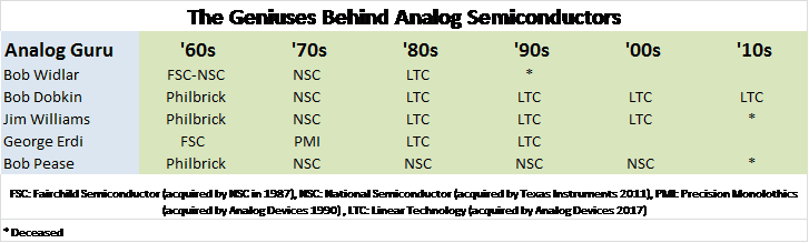
Now, let’s piece together their interwoven connections and how they made the analog semiconductor business what it is today. George A. Philbrick Research is credited with the commercialization of tube based operational amplifiers for analog computers so it isn’t surprising that some of the industry’s top analog IC designers came from this institution. The ‘60s represented a transition of analog design from vacuum tubes to silicon. Fairchild was an early magnet, recruiting Bob Widlar from one of their customers to integrate these tube designs into silicon. Widlar’s μA702 went into production in October 1964. The device set the direction for the industry for decades and at a price of whopping $300. In 1965, his μA709, which followed the μA702, became another technical and commercial success but by then Widlar had moved on the National Semiconductor along with several former Fairchild engineers.
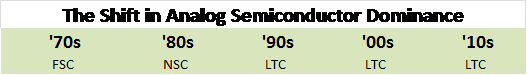
Detailed Bios for each of these folks is available online and worth reading. The interesting thread here is the correlation of their employment history with the change in analog IC leadership. Fairchild almost had a chance but it’s inexperienced management lost critical mass early as resources were deployed to such things as a poorly defined F8 microprocessor video games and digital watches. In the late ‘70s National’s dominance emerged and remained well into the ‘80s. When their core analog team left in the early ‘80s to form Linear Tech, the handwriting was on the wall and National tried unsuccessfully to diversify into markets like memory and processors. Linear Technology built momentum through the ‘80s and ruled the ‘90s, ‘00s and ‘10s (and still does so today, under the guise of Analog Devices) with unparalleled innovation coupled with superior management. (See Table 2 below)
There is an inherent delay between a company’s buildup of an analog team and its emergence as a dominant contender. Standard product analog chips that must work perfectly in hundreds or thousands of different applications take time, upwards of 3-5 years to design and even more time to get designed into systems and ramped to volume production. It takes fortitude and staying power.
Throughout their careers, these Gurus mentored hundreds of engineers who themselves have mentored hundreds more. They are what made these Silicon Valley analog companies so great. It wasn’t UC Berkeley or Stanford University. It wasn’t putting a ton of analog knowledge into a software-defined platform. It was side by side collaboration in an employment environment that was highly mobile. Knowledge spread rapidly. This is where analog is learned and perfected. The disciples of these heroes continue to drive analog IC innovation in Silicon Valley today.
The scope of analog is immense, covering everything that comes into contact with the physical world as either an input or an output and much of what goes on in between. Your application may encompass any combination of complex analog signal chain elements, each of which requires very specific skills and expertise to properly execute into an ASIC chip. When evaluating the analog skills needed for your project, be sure your intended supplier has the matching skilled resources. The more you understand about Analog ASICs the better prepared you will be in selecting the best supplier for your needs.
Occasionally Analog ASIC requirements evolve from existing products using off the shelf analog ICs. The customer is driven to ASIC implementation by a need to lower costs, improve reliability and shrink the size of his product and sometimes to hide his design and thus protect his Intellectual Property. Since the existing solution uses products with public datasheets, preparing a proposal for their integration is somewhat straight forward. Even the pretenders can do that much. Performance parameters for the off-the-shelf components are published and understood. But if the customer desires some performance improvement where even minimal Analog design effort is needed to define and quote the new part, the pretenders often fall flat on their faces and if not during the quote process, then most certainly during execution.
More often, the Analog ASIC requirement is a completely new circuit, perhaps initially envisioned with some off the shelf components, but incorporating considerable invention on the part of the customer and also on the part of the ASIC supplier. Sometimes a spec or partial spec for the system is available as a starting point and maybe a combo schematic / block diagram. Just bidding on such a requirement may require several days or weeks of engineering evaluation, high level design and some simulation to determine if what the customer is requesting is even feasible as was the case with a recent project from a sensor manufacturer. The MEMS pressure sensor was extremely well designed and defined. But the calibration and signal conditioning implementation was a blank slate…almost. The customer’s requirement at first seemed unobtainable. In fact they told us that three of the seven companies they approached had told them so. Critical to the success of the design were the following:
Initially we had to determine if the customer’s request was violating any of the laws of physics, e.g. is it even possible to build such a chip on a single silicon wafer. The customer was skeptical since three companies had already told them so. The challenge was to identify a wafer fab process capable of meeting the design criteria (not all of which are shown above). There wasn’t one. However, thanks to the breadth of knowledge of the ASIC design team, they were able to define modifications that could be made to an existing process that would eliminate the barriers. Meetings were held with the fab’s process engineers who then went back and compiled characterization data to compare with the requests. In one case, noise, the characterization data showed that by using certain new architectures suggested by the design team and confirmed by the fab’s engineers, the tight noise figure could be met without process changes.
The takeaway here is that the ASIC design team knew enough about the fab processes to explore and identify not just the sources of noise, but architectural techniques to minimize its effect on the chip’s performance and thus meet the customer’s expectations.
Once this hurdle was eliminated, the team dismantled the requirements into manageable pieces. A high level block diagram was created (see Figure 2 below) and then each critical section was simulated to verify feasibility.
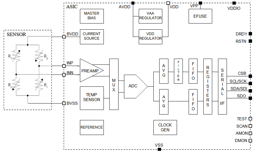
Not only did each block have to be conceptualized at a high level but also an estimate of its area needed to be calculated to determine if the cost budget would be met. Overhead for interconnect area was considered. Architectures were rethought to squeeze out the last 0.001 mm2 of die size. And much of this was done before any contractual development commitment was received from the customer. This is the hidden effort that goes behind a budgetary proposal. During the ensuing weeks, over a dozen conference calls and more than 150 emails were exchanges directly between the design teams (Customer, Foundry and ASIC supplier) to clarify, critique and confirm all aspects of the requirement and its Analog ASIC embodiment, resulting is a thorough and detailed development and production proposal to the customer.
Admittedly, this example was more complex than most, but it offers insight into the work that needs to be done when asked to quote an Analog ASIC.
Some ASIC companies will offer short cuts, suggesting the use of acquired IP and/or cell libraries to save time. Had IP from generic cell libraries been considered in this design, the chip would have failed, having not met many of the performance criteria; especially noise. (An excellent discussion of noise by Intersil can be found here: http://bit.ly/2DaQG89 ) Signal noise can interfere with both analog and digital signals. However, the amount of noise necessary to affect a digital signal is much higher because digital signals communicate using a set of discrete electrical pulses to convey digital “ones and zeros” and those electrical pulses require a lot of noise in order to be confused with one another. Digital designers can’t ignore noise, but in the realm of a mixed signal ASIC or predominantly Analog ASIC, their expertise in sourcing and reducing it are often insufficient. Thoroughly understanding noise, its sources and the proper means of reducing it, comes from decades of experience, not text books.
It is not possible for every Analog ASIC company to have the depth of technical resources to cover 100% of all possible requirements. What is important is that the one you select has as much as possible and has the ability to easily contract the rest. Thanks to the seven decades of analog history discussed above, Silicon Valley has the greater density of contract and semi-retired analog experts in the world that are readily available to supplement an ASIC team.
Two final cautionary thoughts about selecting your Analog ASIC supplier:
It’s not difficult weeding out the analog imposters once you know what to look for.
This is a guest post by Bob Frostholm.
