

One of the most common factors that can have a lasting impact on any given semiconductor device is heat. Any logic circuit or electronic device requires a power supply to drive the function of its parts. While most of this power is used up for basic logic functions and signal generation and transmission purses, part of the electrical energy obtained from the power source is converted into other forms such as heat energy which may heat up the package or be dissipated into the surrounding ambience. Excessive thermal energy in the close environment or poor dissipation of the heat can lead to the activation of several thermal-accelerated processes that damage the package, hinder its performance, or make it non functional altogether. Why should you suffer thermal associated losses when you can just as easily prevent them from causing your electronic circuitry harm?
Why is Thermal Management Essential for Printed Circuit Boards?
When thinking about managing your semiconductor device, one of the aspects you need to cater to is thermal monitoring and management. Modern electronic devices and logic circuits are as complex and dense as they have ever been. With functionality expressed to the maximum, the issue of heat management has become even more relevant today.
As a general rule of thumb, you either want your electronic device to be efficient at heat dissipation, consume as little power as possible to reduce the chances of energy wastage, or be effective at even heat distribution across the whole package. The reason why this is so important is because any electronic circuit has a temperature range within which its components function optimally. If excessive heat energy continues to pool within the package and is not transferred to the environment adequately, it can lead to poor device performance as well as decreased reliability in regards to results.
In order to better understand how you can best address the basic thermal needs of your packages and how you can ideally deal with these commonly arising issues, it is important to familiarize yourself with the fundamental thermal characteristics of any given electronic package. This knowledge and deeper understanding can assist you in making the right decisions when it comes to employing the ideal solutions for your electronic systems and circuits.
Calculating Thermal Resistance
The transfer of heat energy in an electronic package can be explained using simple physics principles like conduction, convection, and radiation. The heat energy generated by the die travels to the active package surface through conduction whereas it is dissipated into the surrounding environment through convection and radiation. Based on this model of heat transfer in an electronic package, we can derive a term and formula to quantify the rate of heat transfer between the two bodies. This is known as the thermal resistance that exists between the die and the surrounding environment.
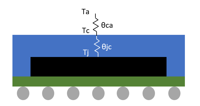
The overall thermal resistance between the die and the environment would include the thermal resistance between the die and the package as well as the thermal resistance between the package surface and the surrounding environments. These thermal resistance factors are represented in the form of theta characters. Each of these two factors plays a critical role in the equations for thermal resistance and are denoted by θjc and θca respectively (where jc stands for junction to case and ca stands for case to ambient). The θja (junction to ambient) thermal resistance can be calculated using the following equations:
θja = θjc + θca
θjc = (Tj – Tc) / P
θca = (Tc – Ta) / P
θja = (Tj – Ta) / P
Where P is the power in Watts that is dissipated by the electronic circuit, Tj is the average temperature of the die, Tc is the average temperature of the package, and Ta is the temperature of the ambient environment.
Junction to Ambient Thermal Resistance
As mentioned above, the junction to ambient or junction to air thermal resistance is a quantification of how well your electronic device is able to remove heat from the active surface of your package and transfer it to the surrounding environment. This value is important when making a comparison between the thermal profiles of two different packages. A calculation can be made to derive the maximum power dissipation that can be allowed in a package using the following formula:
Maximum Power Allowed = Maximum junction temperature – Maximum ambient temperature / θja
Ideally, the power consumption of the device should be lower than the above calculated value for the maximum power dissipation allowed in the package. In the case that the actual power consumption of the package is higher than the maximum allowed power dissipation, then there is a need to introduce some form of a solution that would improve the heat removal process, such as using a heat spreader to improving the airflow inside the package to facilitate the thermal dissipation.
Junction to Case Thermal Resistance
The junction to case thermal resistance, on the other hand, is the measure of the capability of the package to transfer thermal energy from the die to the active surface of the package, top or bottom. It can be calculated using the following formula:
θjc = (Tj – Tc) / Pjc
The key is to make sure that the junction temperature of the device always remains below the maximum power allowed value as it improves design reliability and makes it more robust. Apart from that, there is also the need to employ the use of effective dissipating solutions that facilitate the outflow of heat through the integrated circuit and transfer it to the ambient to prevent overheating. Using these parameters enables engineers and circuit designers to extend the lifetime of logic devices and make them much more reliable in the long run. The above mentioned formulas allow them to calculate or estimate various kinds of thermal resistance found in packages which, in turn, helps to optimize device performance and metrics.


