

With a rapid progression in the applications involving artificial intelligence, data generation has been increased exponentially in last few years. It has been estimated that in 2018, 2,5 quintillion bytes of data is generated every day [1]. This huge data generation puts enormous computational requirements on telecom platforms and data centers which are then putting a significant pressure on the advancements in manufacturing of such high-speed circuits to transport/process this data. With traditional chip manufacturing approach reaching its physical limitations, other approaches to create/manufacture such integrated circuits have been investigated, silicon photonics being one of them.

Silicon photonics is rapidly developing and emerging industrial field. In very short time, this field has gone from “hot research topic” to an industry viable manufacturing process. The reason this technology is getting a lot of traction is the fact that industry can use already developed and matured platforms/tools used in CMOS fabrication that are used today to manufacture electronic chips. The photonics chips sometimes also called light chips are fabricated using different materials such as Lithium Niobate, high index glasses and nitrides, polymers, and Silicon. The advantage of using same manufacturing platforms as CMOS based silicon devices is high yield and potentially much lower cost per device.
In optical chips, there is waveguide. Waveguide is a wire that propagates light from one end of the chip to the other. We can think of waveguide in silicon photonics as a very scaled down version of optical fiber. Silicon is used to fabricate this waveguide in silicon photonics. Silicon has a high refractive index of 3.5 and it is surrounded by glass (silicon-oxide) on all sides, which has low refractive index 1.45. The waveguide core (Si) has a higher refractive index than cladding (silicon-oxide).This higher difference between core and cladding helps to fabricate waveguides with very small size, typically 500 nm wide and 220 nm high. There is another advantage of this high refractive index contrast that light is tightly confined inside the core which helps in fabrication of waveguide with bend radius of 1 or 2 micrometers. We can create passive devices, photodetectors, moderators etc. with these waveguides. We can use Si waveguides on silica (silicon dioxide) in the wavelength range just above 1 micron to 4 micron, in the transparency region of silicon. If we want to work in other wavelength ranges, we need to use other materials as waveguide core. For example, we can use silicon nitride in the visible part of the light spectrum, and we can use germanium if we want to go deep into the infrared by using the already established CMOS fabrication facilities.
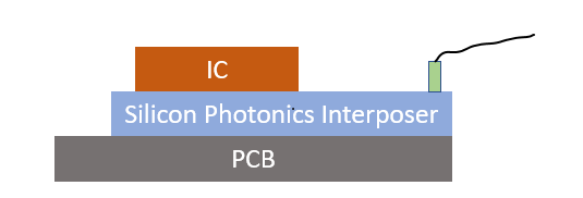
Silicon photonics circuits are fabricated using a silicon substrate (wafer) as a base. Then there is 2-to-3-micron high layer of silicon oxide (BOX- buried oxide). This layer acts as an insulator as it is a low index layer that separates the silicon substrate from the silicon layer, where all the action is happening, residing on top of BOX. The height of Si layer is around 220 nm. A coating of photosensitive resist is put on top of the Si layer to create patterns. Electron beam can be used to imprint a pattern in the photosensitive resist. The resist is developed, and exposed areas of Si are etched away by using reactive ion etching. Shallow etch is used to create grating fiber couplers to guide the light from/to optical fibers and deep etch is used to create waveguide structures. In order to have active function like modulation, pn junction can be made inside Si waveguide. The carriers can be pulled out or injected into the pn-junction by applying voltage, which modulates the refractive index and allows to do modulation. To achieve detection inside a silicon photonics chip trick is to epitaxially grow germanium on silicon, as Germanium absorbs the telecom wavelengths. In silicon photonics, unfortunately there is no trick to make silicon emit light at telecom wavelengths and to be used as light source. The approach that is commercially used is to bond III-V materials to Silicon and then process a laser in it. Research is moving in direction to epitaxial grow III-V materials on silicon.
To achieve a working chip goal, there are number of steps to follow. The first step is to get an idea and next step is to translate that idea into a circuit diagram. Once there is circuit diagram, we need to simulate the circuit. After successful simulation of the circuit, we need chip layout to be sent to foundry for fabrication. After fabrication, we need to test the chip. For example, we build an optical transceiver. We need to design, fabricate, package, and test it before we actually know it works. This whole process from design, fabrication and testing takes between 9 months to 12 months. There is a factor of variability in the photonic integrated circuits. The Si waveguides are sensitive to nm scale variations. A one nm change in width of Si waveguide during fabrication process can shift the photonic integrated filter response by 1 nm in wavelength. This variability can be handled by moving from fixed circuit elements to tunable circuit elements.
Silicon photonics has applications ranging from optical communication to life sciences. Websites are housed in data centers all around the world and in data centers several 1000s of servers are needed to be interconnected. The lengths of these interconnects can be from meters to few hundred meters with data rates of up to 100 Gigabits/second. It is economically not feasible to make these interconnects electrical at these high data rates. All these interconnects today are optical using the optical fiber technology and silicon photonics is the technology used to convert electrical signals into optical signals and vice versa. This function is performed by silicon photonic modulator with typical data of 100 Gb/sec and typical symbol rate of 25 GigaBaud in various modulation formats. There is ongoing research to develop modulators with data rate of 400-800 Gb/sec and symbol rate of 50-100 Gb/sec.
Silicon photonics has applications in the field of medicine and health as we can fabricate low-cost optical chips with very high sensing capabilities, even for some cases the chips can be used as disposable devices for one-time use only. We can fabricate such compact devices that can be used for body implants. Main applications of silicon photonics in medicine can be characterized in four categories, in-vitro diagnostics, smart pills, wearables, and point-of-care (POC) medical devices. Silicon photonic biosensors can be used for viral infection diagnosis using the genomic detection, antigen-directed virus detection and serological test method. Commercial example is Genalyte, California based company, COVID-19 multi-antigen serology panel that uses silicon photonics chip based optical ring resonance technology to perform tests on small volume of blood.
References:
[1]. Seed Scientific


