

If you are involved in any ASIC/SOC design life cycle, it is highly likely that you would have heard questions like – Have you verified a feature? Is all feature testing completed? How will you validate a new feature? What design defects were found and how?
The terminologies Verification, Validation and Testing are used interchangeably and can be confusing at times- at least for entry level engineers.
All of these terms does relate to testing of the chip but refers to the same at different stages in a chip design and manufacturing flow. Here is what they really mean.
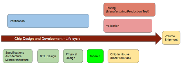
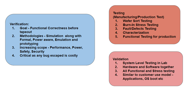
SoC Verification is a process in which a design is tested (or verified) against a given design specification before tape-out. This happens along with the development of the design and can start from the time the design architecture/micro architecture definition happens. The main goal of ASIC verification is to ensure functional correctness of the design before the tape out. However with increasing design complexities, the scope of verification is also evolving to include much more than functionality. This includes verification of performance and power targets, security and safety aspects of design and complexities with multiple asynchronous clock domains. Simulation of the design model (RTL) remains the primary vehicle for verification while a lot of other methodologies like Formal property verification, Power-aware simulations, emulation/FPGA prototyping, static and dynamic checks etc also are used for efficiently verifying all aspects of design before tape out. The ASIC verification process is considered very critical as part of design life cycle as any serious bugs in design not discovered before tape-out can lead to the need of newer steppings and increasing the overall cost of design process.
SoC Validation is a process in which the manufactured design (chip) is tested for all functional correctness in a lab setup. This is done using the real chip assembled on a test board or a reference board along with all other components part of the system for which the chip was designed for. The goal is to validate all use cases of the chip that a customer might eventually have in a true deployment and to qualify the design for all these usage models. Validation happens initially for individual features and interfaces of the chip and then can also involve running real software/applications that stress tests all the features of the design. Validation team usually consists of both hardware and software engineers as the overall process involves validating the chip in a system level environment with real software running on the hardware.
There are some companies that use the term Validation in a broader perspective and classifies the activities before and after Silicon/chip availability. Verification hence is also referred to as Pre-Silicon Validation (indicating activities before the silicon chip is available) and Validation is also known as Post-Silicon Validation.
SoC Testing (Manufacturing/Production test) involves screening manufactured chips for faults or random defects, reliability, functional defects and electrical characterization before volume shipment.
The first level of testing happens on a wafer level before individual dies are packaged. This is known as Wafer sort/probe testing that characterizes the various technology and transistor parameters before the die is cut out. This step helps in identifying faulty dies before packaging.
The next level of testing happens on a packaged die to stress for reliability by testing at increased temperatures and identifying chips that can fail easily. This process is known as burn-in stress testing.
The third level of testing is used to identify manufacturing defects or faults. At a high level this process involves stimulating the input ports with various test patterns (also known as test vectors) and comparing the output responses against expected results. Tester equipments like ATE (Automatic Test Equipment) are used which can take individual chips and run IC testing, with test pattern stimulus and response checked automatically.
The next level of testing is to characterize and screen chips before volume shipments. Characterization involves testing the design with voltage and frequency shmooing to find the ideal operating conditions. Designs with high speed IOs (like PCIE, Ethernet, DDR etc) also goes through characterization of IO ports by shmooing various electrical parameters to arrive at ideal transmission and error rates.
Functional defects are identified in the parts using functional test patterns. These functional test patterns are identified to exercise the different parts in a chip to achieve satisfactory coverage and run at actual speeds.
To summarize here is a quick summary of what each of these steps include:
For more related topics and questions on Verification/VLSI, do refer to my Quora profile – https://www.quora.com/profile/Ramdas-Mozhikunnath
