

Wafer probe (or wafer probing) refers to the electrical testing of semiconductor dies while they are still part of the wafer. By using microscopic probe needles to contact bond pads or built-in test points on each die, engineers can:
Unlike packaged device tests, wafer probing occurs at the wafer level—offering rapid, cost-effective feedback during fabrication without the expense of packaging bad dies.
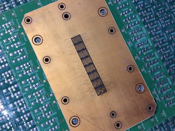
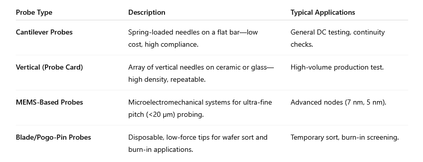
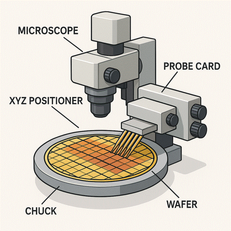
A modern wafer probe station consists of:
Estimate NRE for test development and an indicative per-unit test cost.
Wafer Loading: Operator or robotic handler places wafer into cassette, loads onto stage.
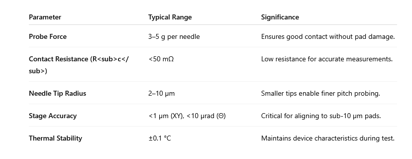
Calibration & Alignment:
Thermal Conditioning: Ramp to test temperature for stress or performance characterization.
Probing Sequence:
Data Collection & Analysis:
Wafer Sorting: Map bad dies for exclusion during dicing; generate wafer map for downstream processing.
Needle Wear & Breakage:
Pad Damage (“Scriber” Marks):
Electrical Noise & Crosstalk:
Poor Thermal Uniformity:
Low Throughput:
Q1: What’s the difference between wafer probe and final test?
A: Wafer probe tests dies on the wafer before dicing. Final test occurs after packaging to validate external interconnects, sealing, and mechanical integrity.
Q2: How often should probe needles be replaced?
A: Dependent on material and usage, but typically every 5,000–10,000 touchdowns. Monitor contact resistance and visual tip wear to fine-tune replacement intervals.
Q3: Can wafer probing detect latent reliability issues?
A: Basic DC/AC tests may not reveal all latent defects. Integrating ESS modules or burn-in steps can screen for electromigration and early-life failures.
Q4: How do I reduce wafer probe cycle time?
A: Optimize test vectors (e.g., parallel testing of multiple pads), employ handler automation, and leverage vector compression and abort-on-fail strategies.
