What Is Wafer Testing?
Wafer testing—often called wafer sort or probe testing—is the process of electrically evaluating individual semiconductor dies directly on the wafer. Using precision probe needles to make contact with bond pads or dedicated test structures, wafer testing allows engineers to:
- Verify Device Functionality: Confirm logic, analog, RF, or memory blocks operate per specification.
- Characterize Parametric Performance: Measure leakage currents, threshold voltages, timing margins, capacitance, and more.
- Screen Out Defective Dies: Identify process-induced defects, contamination, or latent reliability issues before expensive packaging steps.
- Feed Back to Process Control: Provide early data for statistical process control (SPC) to fine-tune fabrication equipment and processes.
By detecting failures at the wafer level, manufacturers save substantial packaging and assembly costs—only high-quality dies progress to final test and shipment.
Why Wafer Testing Matters in Semiconductor Fabrication
- Cost Reduction: Packaging and assembling a bad die can cost 10×–100× more than probing it on-wafer. Early discard prevents downstream waste.
- Yield Improvement: Wafer-level data pinpoints process drifts or excursions, enabling rapid root-cause analysis and corrective actions.
- Time-to-Market Acceleration: Fast feedback loops shorten debug cycles, reducing tape-out iterations and speeding product rollout.
- Reliability Assurance: Screening for marginal or latent defects (via burn-in or stress tests) boosts field reliability.
- Design Verification: On-wafer functional tests validate new design IP across process corners before committing to full wafer fabrication.
A robust wafer testing strategy underpins every high-performance fab’s success—directly translating to higher yields, quality, and profitability.
Types of Wafer Tests
Wafer testing encompasses multiple test categories, each targeting different failure modes:
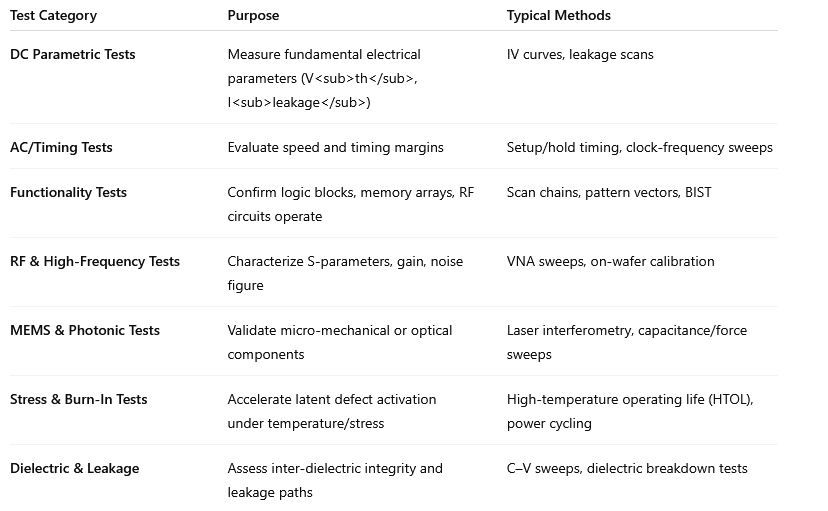
Mixing these tests into a coherent wafer sort flow ensures comprehensive coverage of all critical failure mechanisms.
Wafer Testing Workflow & Process Flow
A typical wafer testing sequence follows these steps:
Wafer Preparation & Loading
- Clean wafer to remove particles.
- Load wafer into probe station via cassette or robotic handler.
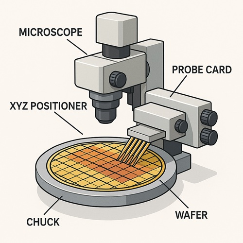
Alignment & Calibration
- Use fiducial marks and optical microscope to align X, Y, Z, and θ axes.
- Calibrate probe needle positions and touchdown heights.
Thermal Conditioning
- Ramp wafer to target test temperature (–60 °C to +150 °C) for stress or performance characterization.
- Allow thermal stabilization before contacting.
Probe Contact & Test Execution
- Approach: Move needles microns above wafer surface.
- Contact: Gentle touchdown; monitor contact resistance.
- Run Test Vectors: Execute parametric, functional, and high-frequency tests per test plan.
Data Acquisition & Storage
- Record pass/fail flags, parametric values, RF parameters, and logs.
- Transfer data to MES/SPC systems in real time.
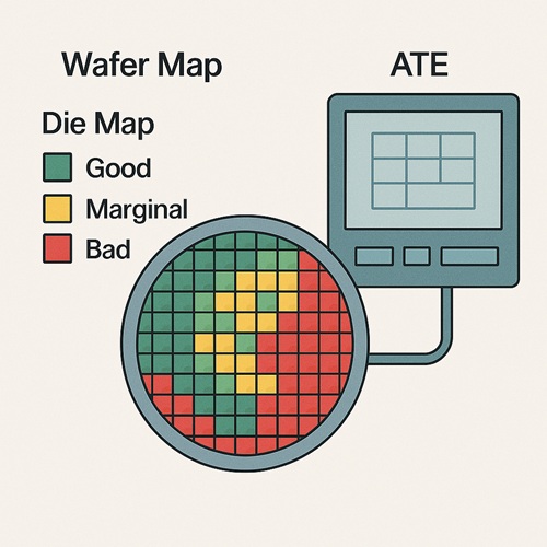
Wafer Mapping & Sorting
- Generate die map: mark good versus bad dies.
- Export wafer map for dicing saw to avoid bad die packaging.
Feedback & Analysis
- Feed data into SPC tools to track trends, detect excursions, and trigger corrective actions.
- Use root-cause analysis for systematic failures.
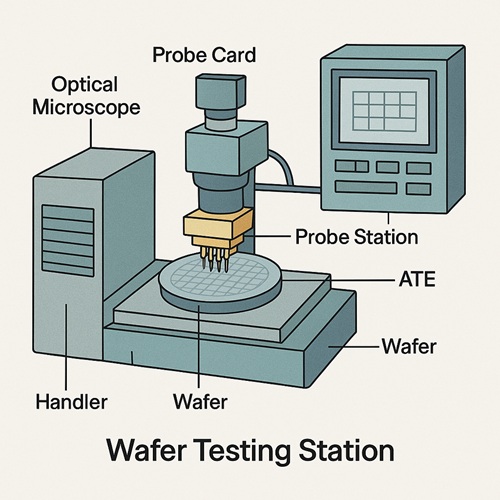
Key Wafer Testing Equipment
High-volume, high-precision wafer testing relies on specialized equipment:
Probe Station / Handler:
- Manual or fully automated stages.
- Temperature-controlled chuck (–60 °C to +300 °C).
- XYZΘ motorized stages with sub-micron accuracy.
Probe Cards & Needle Technologies:
- Vertical, cantilever, MEMS, or specialized RF probe cards.
- Tip geometries optimized for pad pitch (down to <20 µm).
- Floating liquid metal or spring probes for ultra low-force contact.
Automatic Test Equipment (ATE):
- High-performance test instruments (parametric analyzers, digital pattern generators, RF VNAs).
- Multi-site testing capability to probe dozens-to-hundreds of dies simultaneously.
Vision & Alignment Systems:
- High-resolution cameras with fiducial detection.
- AI-driven alignment for rapid, automated needle positioning.
Data Management & SPC Software:
- Real-time data acquisition, yield analytics, and trend monitoring.
- Integration with MES, LIMS, and factory data fabric.
Test Program Development & Methodology
A well-designed test program balances coverage, speed, and cost:
Design-For-Test (DFT) Integration
- Incorporate scan chains, built-in self-test (BIST), and boundary-scan ports at the design stage.
- Adds test points for critical nodes, reducing vector count.
Test Vector Optimization
- Use vector compression or abort-on-fail strategies to minimize per-die test time.
- Partition tests: execute quick DC checks first, proceed to more time-intensive RF/functional only on passing dies.
Multi-Site Testing
- Probe multiple dies in parallel to multiply throughput.
- Ensure ATE supports synchronized test flows and independent site control.
Thermal & Stress Profiling
- Define thermal cycling or burn-in profiles that uncover latent defects without overstressing good devices.
- Balance burn-in time and throughput constraints.
Continuous Test Improvement
- Analyze first-pass yield (FPY) and defect densities to refine test limits and coverage.
- Update test recipes based on SPC alarms and failure analysis feedback.
Data Analysis, Yield Optimization & SPC
Leveraging wafer test data unlocks yield gains:
Statistical Process Control (SPC):
- Monitor key parameters (V<sub>th</sub>, leakage, contact resistance) over time.
- Implement control charts and Cpk analysis to detect drift and out-of-control conditions.
Wafer Map Analysis:
- Visualize spatial defect clustering to identify equipment or process zone issues.
- Correlate probe map patterns with fab tool data (e.g., lithography, etch, CMP) for root-cause.
Yield Learning Loops:
- Link wafer sort failures to package/test yields.
- Adjust sort-limit margins to balance wafer-level yield versus packaged device reliability.
Machine Learning & AI:
- Predict wafer yield based on early probe data.
- Optimize test sequences dynamically to maximize throughput and coverage.
Common Challenges & Troubleshooting in Wafer Testing
Probe Needle Wear & Contact Failure
- Symptom: Rising contact resistance, false fails.
- Mitigation: Schedule tip inspection/replacement cycles; use hard-coated tips for abrasive wafers.
Wafer Warpage & Alignment Drift
- Symptom: Inconsistent touchdown heights, pad scratching.
- Mitigation: Employ vacuum-backed chucks with backside fluid cooling; real-time autofocus alignment.
Electrical Noise & Crosstalk
- Symptom: Fluctuating measurements, false parametric failures.
- Mitigation: Use shielded cabling, minimize loop areas, implement Kelvin sensing where possible.
Low Throughput & High Test Cost
- Symptom: Bottlenecks at probe stations, rising cost per die.
- Mitigation: Increase multi-site count, optimize vector sequences, deploy handler automation.
Data Overload & Analysis Lag
- Symptom: Delayed SPC alarms, missed excursions.
- Mitigation: Streamline data pipelines, adopt in-memory analytics, prioritize key metrics.
Best Practices for High-Yield Wafer Testing
- Standardize Recipes & Workflows: Maintain centralized libraries of probe card setups, test programs, and alignment recipes.
- Preventive Maintenance Scheduling: Automate cleaning, calibration, and tip replacement based on usage counters.
- Cross-Functional Root Cause Teams: Combine fab, test engineering, and failure analysis for rapid turnaround on anomalies.
- Data-Driven Continuous Improvement: Tie wafer test metrics to packaged device yields and field returns for holistic quality control.
- Operator Training & Certification: Regularly update training on new probe technologies, alignment software, and data analysis tools.
- Scalable Automation: Invest in wafer handlers, robotic wafer transfer, and AI-based alignment to remove manual bottlenecks.
Frequently Asked Questions (FAQs)
Q1: How does wafer testing differ from packaged device test?
A: Wafer testing evaluates dies on-wafer before dicing and packaging, focusing on die-level functionality and parametrics. Packaged device tests assess final assemblies, including wire bonds, seals, and external interfaces.
Q2: What are the main cost drivers in wafer testing?
A: Packaging costs of bad dies, probe station throughput (site count), ATE rental or capital, probe card maintenance, and test program development.
Q3: How often should probe needles be replaced?
A: Replacement intervals vary by tip material and usage but typically every 5,000–15,000 touchdowns. Monitor contact resistance and visually inspect tip wear to tune cycles.
Q4: Can wafer testing detect all possible defects?
A: While comprehensive, wafer testing may miss latent reliability issues. Adding stress-screening (burn-in, HTOL) and environmental tests improves coverage.
Q5: What role does data analytics play in wafer testing?
A: Advanced analytics and AI help predict failures, optimize test sequences, and correlate wafer-level data with packaged yields—driving continuous yield improvement.


