

Wafer fabrication, or wafer fab, plays a crucial role in transforming raw materials into the intricate microchips that power everything from smartphones to electric vehicles.
The process of wafer fabrication involves various sophisticated techniques and technologies that ensure precision and efficiency in creating integrated circuits. With the growth of applications across multiple sectors, understanding the complexities of wafer fab is essential for comprehending the larger landscape of technological innovation.
This article will explore the fundamentals of wafer fabrication, highlighting its processes, end-user applications, and the impact of Industry 4.0. We’ll also delve into the challenges and future trends that shape this vital industry, illustrating its significance in our rapidly evolving digital era.

A wafer fab, short for wafer fabrication, is a manufacturing plant where semiconductor wafers are created. These wafers are thin slices of semiconductor material, like silicon, used in the production of electronic devices. The process involves several precise and complex steps to produce functional chips.
Wafer fabs are crucial for companies in the semiconductor industry, such as Intel Corporation. They are responsible for the production of semiconductor components used in everything from phones to computers.
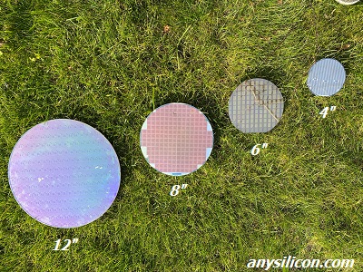
To meet the growing demand for semiconductors, especially from 2015-2021, wafer size and product quality have become a primary focus. As we look to the foreseeable future, wafer processing will remain a vital part of technology development, driving semiconductor industry revenue growth.
Wafer fabrication is the heart of semiconductor manufacturing. This process turns raw materials into complex electronic circuits. Each step must be precise to ensure high-quality chips. From cleaning the silicon to creating detailed circuit patterns, each stage is crucial.
Photolithography is a core technique in fab labs. Here, light projects patterns onto silicon wafers, defining circuit designs. This step involves layers of light-sensitive material and precise light exposure. The result is a detailed and accurate pattern crucial for the chip’s functionality.
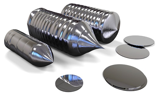
The journey begins with silicon. This raw material is shaped into large, thin slices known as silicon wafers. These wafers are the foundation for all semiconductor devices. They undergo cutting, cleaning, and polishing to ensure smooth surfaces for further processing.
Imprinting integrated circuits onto silicon wafers involves several detailed steps. After photolithography, etching removes unnecessary material. Doping introduces impurities to alter electrical properties. Planarization smooths the wafer surface, prepping it for later stages. Each phase adds complexity to the circuits.
![]()
Once wafers are processed, testing and quality assurance begin. This step ensures that each chip functions correctly. Advanced machinery tests electrical performance and checks for defects. Quality assurance is key to producing reliable semiconductor components that power modern technology.
—
The semiconductor industry is crucial to various sectors. The demand for semiconductors is rising, driven by the needs of automotive, consumer electronics, and industrial applications. This demand impacts semiconductor revenues and revenue growth. In these fields, silicon wafers and the semiconductor manufacturing process play key roles. Integrated device manufacturers compete to innovate in wafer fab technology.
In the automotive sector, semiconductors are vital for building modern vehicles. They power complex circuitry for features like driver assistance and in-car entertainment. Semiconductor fabs produce components that ensure functional chips for improved vehicle safety and performance. As the demand for semiconductors grows, so does the need for advanced wafer processing steps to meet the industry’s high standards.
Consumer electronics rely heavily on semiconductors for innovation. From smartphones to smart TVs, these devices use chips formed on silicon wafers. During the 2015-2021 period, the demand for technology stocks surged, pushing semiconductor industry revenue growth. This sector depends on the wafer fab’s ability to create chips with consistent product quality and varied wafer sizes to fit diverse gadgets.
In industrial settings, semiconductors enable automation and efficiency. They are crucial in creating electronic devices that manage everything from energy systems to manufacturing lines. Intel Corporation and other integrated device manufacturers focus on developing semiconductors that withstand rigorous conditions. Their proprietary semiconductor industry model ensures these chips perform optimally, even under a slower rate of technological change.
A focus on air shower environments and cycle basis in wafer fabs ensures these chips meet industry needs. As the world advances, the future of computing in these applications hinges on continuous innovation in semiconductor components.
The fourth industrial revolution, known as Industry 4.0, is transforming wafer fabs. Wafer fabs are facilities where silicon wafers are made. These wafers are critical for semiconductors, which are vital for electronic devices.
Industry 4.0 introduces advanced technologies like artificial intelligence and the Internet of Things. These technologies help improve the semiconductor manufacturing process. By using smart sensors and data analytics, Industry 4.0 enhances product quality and efficiency.
Here is how Industry 4.0 impacts wafer fabs:
– Real-Time Monitoring: Sensors collect data during wafer processing steps. This data helps in making faster decisions.
– Predictive Maintenance: AI helps predict equipment failures before they happen, reducing downtime.
– Increased Automation: Robotics and automation reduce human error and increase precision.
– Supply Chain Optimization: Smart systems manage the demand for semiconductors, aligning production needs.
Industry 4.0 is a primary driver for change in conventional wafer fab processes. It aligns with the future of computing by ensuring better silicon wafers. Consequently, semiconductor industry revenues are likely to grow at a slower rate, but with more stability and quality.
In summary, Industry 4.0 is revolutionizing wafer fabs, ensuring they meet the technological demands of the foreseeable future.
The semiconductor industry relies heavily on skilled personnel for successful wafer fabrication. Skilled workers are essential in several areas of the semiconductor manufacturing process. They ensure product quality and efficiency, which are primary drivers for semiconductor industry revenue growth.
– Wafer Processing: Technicians and engineers monitor wafer processing steps to meet strict standards.
– Complex Circuitry Design: Experienced designers create intricate semiconductor components.
– Quality Control: Workers perform rigorous tests to maintain high-quality semiconductor wafers.
In the foreseeable future, skilled labor will continue to be vital. As semiconductor fabs evolve, the need for trained personnel will grow, influencing future industry trends and integrated device manufacturers like Intel Corporation.
The wafer fabrication landscape is set to undergo significant changes in the coming years. This evolution is driven by advancements in technology and the demand for semiconductors. Key trends include the adoption of new materials and more precise techniques. These trends aim to enhance the performance and quality of integrated circuits while addressing the semiconductor industry’s ongoing growth.
Efforts towards sustainability are growing in wafer fabrication. Companies are focusing on reducing their environmental footprint by:
– Energy Efficiency: Implementing energy-saving measures and utilizing renewable energy sources in fabs.
– Waste Reduction: Recycling materials and minimizing waste at each stage of the wafer processing steps.
– Water Conservation: Using innovative water treatment solutions to reduce water consumption during chip manufacturing.
These efforts not only help in conserving resources but also play a role in maintaining product quality throughout the complex circuitry design processes. As the demand for semiconductors continues to rise, sustainable practices will become a primary driver for integrated device manufacturers and will shape the future of wafer fabs.
The wafer fabrication industry is crucial to the semiconductor sector. It creates the silicon wafers used in making functional chips for electronic devices. However, this industry faces several challenges.
These barriers will shape the industry’s future in the foreseeable future.


