

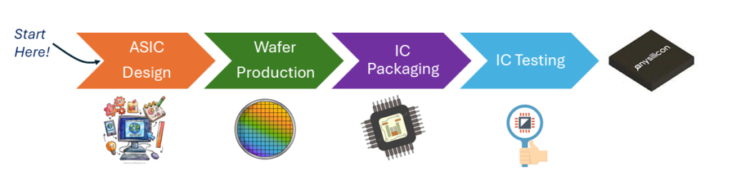
ASIC stands for Application Specific Integrated Circuit — or in other words a chip that is being designed for a specific task.
Those Integrated Circuits (IC) are usually a combination of Analog circuit such as clock, amplifier and denoising circuit and Digital Block such as multiplexers, registers, arithmetic logic units (ALUs), and computer memory. Basically Digital plane is being used for discrete signals [1,0] and Analog is being used for continuous signals (1–0).
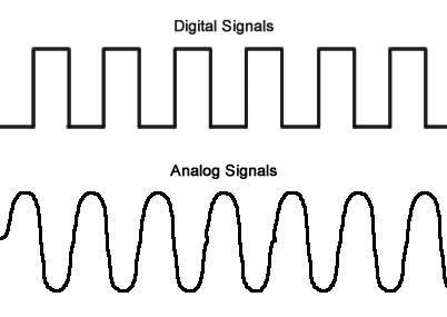
Figure 1: Digital signals vs. analog signals
Let’s say our input signal supposed to look like a rectangle (Digital signal) and we added some noise on top of that signal we can now notice that the Signal with noise is no longer 1/-1 it is actually get up to 2 and down to -2. So with simple filtering (Analog design circuit) we can now see we managed to get the noise signal to something similar to the original.
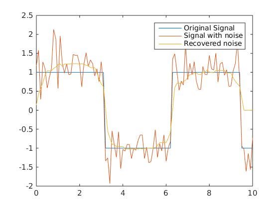
Figure 2: Signal with noise
We will need Digital design circuits, for example, to add 2 digital signals together.
Let’s assume we have 2 black boxes. 1 black box can multiply the 2 input and the other one can do the say “I’ll let you pass only if one of you will be 1 and the other 0”. The first Black Box is called AND gate and the other one is called XOR. Hopefully, you can now understand the table below, we just have 1 more question to answer. 1+1=2 right? I don’t think so :) 1+1=10 we are in the binary world, after all, 10 = 0010, and turning a binary number to decimal is 0*2³+0*2²+1*2¹+0*2⁰=2. Seems okay now right? So we actually managed to get the following now: A+B = CS *** explain in words ***
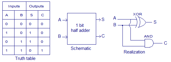
Figure 3: Half adder
Okay, we managed to get an intuition of what is a Digital plane and what we can do with that and hopefully intuition for what is an Analog plane. These two planes are designed by different people and it may take months to design a large ASIC.
During the development of ASIC, we keep on mixing those 2 planes in order to get the fastest and the most power-efficient chip oriented for mining.
Now let’s discuss how we design Digital circuits and how we design Analog circuits.
In digital circuit design, we have 2 main steps, Front-End step where we take a code and synthesize a schematic (netlist) out of it and the second is the Back-End step where we take the netlist and design the layout, in other words, a schematic where each gate will be placed and how we connect them.
The Front-end Designer or Register-Transfer Level (RTL) designer, develops the design while using Field Programmable Gate Arrays (FPGA) or Simulation programs and programmed using Hardware Description Language (HDL) usually Verilog/VHDL.
FPGA? A Field Programmable Gate Arrays an integrated circuit designed to be configured by a customer or a designer after manufacturing. In other words, you can upload your code into it and start debugging.
HDL? hardware description language (HDL) is a specialized computer language used to describe the structure and behavior of electronic circuits, and most commonly, digital logic circuits.
HDL languages are unique because they are being synthesized into logic gates and connectivity between those logic gates and also for each component we design we have to give the Ports. So actually it might be similar to other computer languages but you construct and write in a different mindset. The output of the step is called a netlist, which is the text file of the synthesized logic gates and connectivity.
An example to a VHDL code of the digital block we designed and saw before:
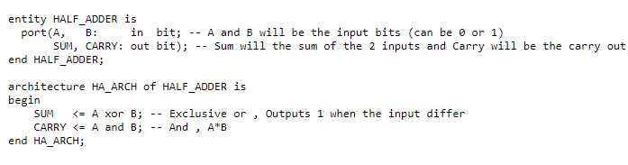
Figure 4: VHDL code example of an Half Adder
In this example we see 2 sections, the first one is the entity and the second one is the architecture. In the entity part, you write the input and output signal names and what kind of data type is it. In the architecture we write down the connection between the input and output.
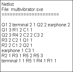
Figure 5: netlist example
An example to a netlist (the output of this step).
The first column is usually the type of the device and name then the connectivity and the last column is actually the multiply of this device.
The second step is called Back-end or physical design. At this step, circuit representations of the components (devices and interconnects) of the design are converted into geometric representations of shapes which, when manufactured in the corresponding layers of materials, will ensure the required functioning of the components. This geometric representation is called integrated circuit layout. This step is usually split into several sub-steps, which include both design and verification and validation of the layout.
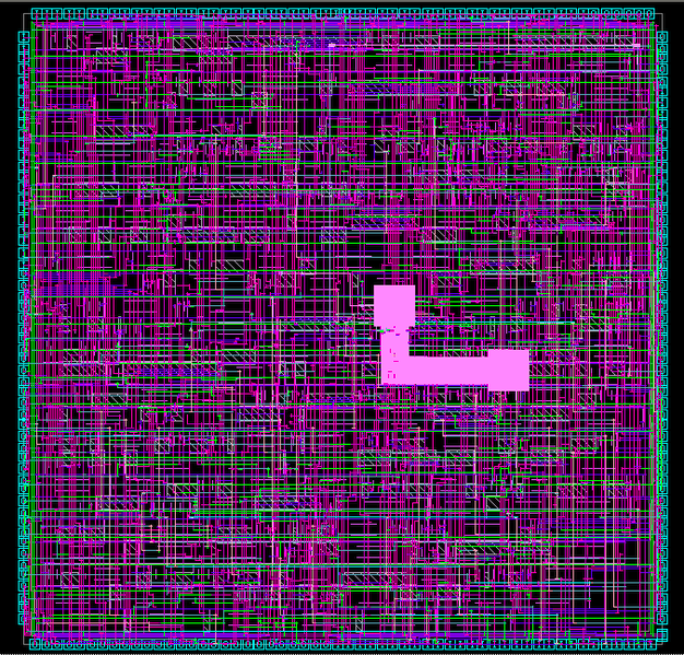
Figure 6: Layout of SHA-256 Accelerator Core
The first step in the analog design is the analog circuit design/schematic design, the designer places devices like resistors, capacitors, inductors and transistors and later on simulate the design with different inputs and samples the output. Most of the design here is made by hand using design tools such as Virtuoso. We cannot translate into RTL code the design here because we are not facing a binary issue here. We are facing issues such as amplification and noise filtering.
The output of this step is a netlist similar to the output of the Front-end.
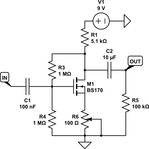
Figure 7: Common source amplifier schematic
The second step is a physical design it is very similar to the Back-end steps in the digital plane. But in this step, some of the routing and placement is done manually at the moment because of analog signals. In general analog signals might be more sensitive to parasitic capacitance and resistance.
Parasitics are additional resistance and capacitance which we didn’t see while we designed the analog circuit. Those parasitics will always appear but sometimes they appear from wrong floor-planning such as placing 2 devices far away from each other or such as placing a sensitive circuit next a to really big capacitor which might cause unwanted capacitance on the circuit next to it. Such parasitic avoidance will result in a floor plan constraint which most of us will see only in the analog plain instead of the digital. The output of this step is called Masks, similar to the output of the Back-end.
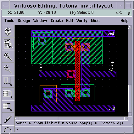
Figure 8: Inverter layout design
The last step in ASIC creation is manufacturing. I’ll divide it into 3 processes Mask making, Wafer making, and Cutting. But first, a few definitions.
Wafer — also called a slice or a substrate is a thin slice of crystalline silicon. The wafer serves as the substrate for microelectronic devices built-in and over the wafer and undergoes many microfabrication process steps such as doping or ion implantation, etching, deposition of various materials, and photolithographic patterning.
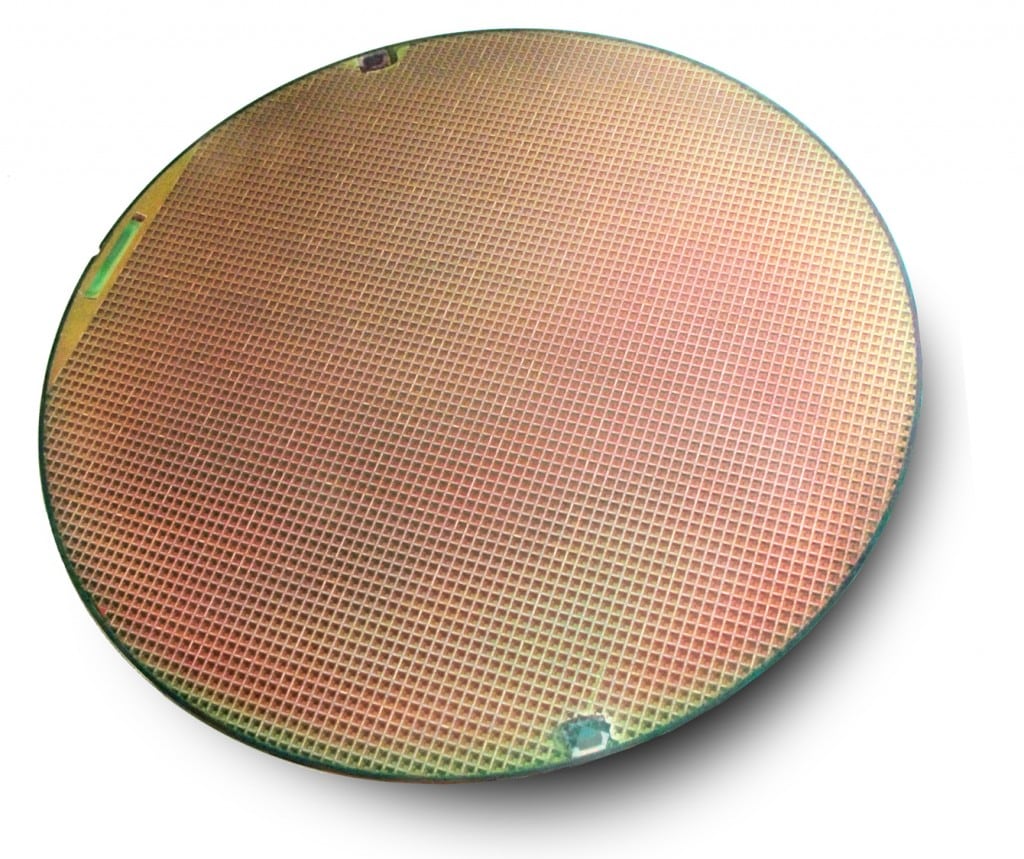
Figure 9: Silicon Wafer
Mask — Unlike the masks we know in those masks we uncover the places we want to print in them very similar to stencil. But instead of painting, we use the microfabrication process steps we mentioned before.
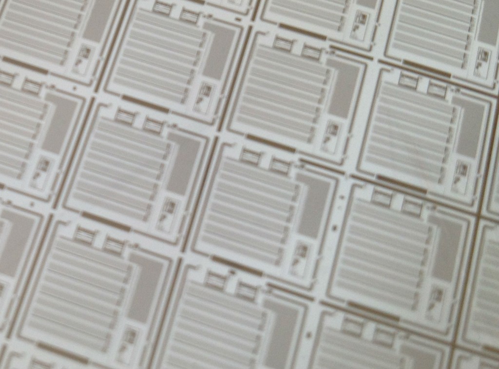
Figure 10: Metal mask for semiconductor manufacturing
Mask making — We take the layout design (plan for the masks) from the Digital and Analog plane merge them and then creating a mask for each layer. What are layers? There are many layers in each ASIC design but I’ll give you an example for two of them. The first one is called Via mask/Interconnect and the other is a Metal mask. Via mask is creating holes in specific places in order to inject metal so I could connect between 2 metals and the Metal mask is where you print the metal.
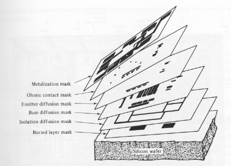
Figure 11: ASIC masks for the lithography process
Wafer making — We take the masks and using different microfabrication process steps on each mask we started creating the ASIC (Each layer at a time). On each wafer, we create a couple of ASICs simultaneously
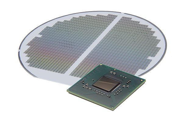
Figure 12: Wafer with hundreds of ASICs
Cutting — The last step is cutting/dicing the ASICs on the wafer.
Figure 13: ASIC in final package
We are now ready for packaging and send out the ASIC.
Get a fast indicative cost range, then unlock a full breakdown by email.
_________________________________
This is a guest post by Adi Szeskin.
