

In June 2021, Google replaced millions of Intel’s CPU with home grown chips. This article provides and overview of the new ASIC developed by team Google to help optimizing the performance of YouTube servers. A custom-made ASIC (chip) rather than a general purpose ASIC (CPU), is design specifically by Google to perform a number specific tasks faster. In this article we will explore the world of ASICs and learn about their types and benefits.
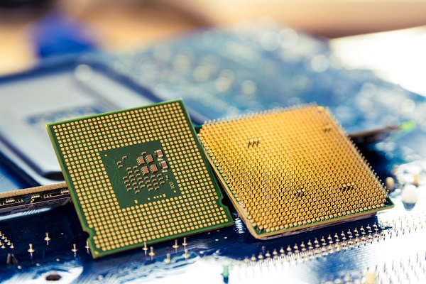
Figure 1 – An example of an ASIC
An application-specific integrated circuit, or ASIC for short, is a chip created for a particular use or application, rather than for general-purpose use. They are usually made using silicon technology. Because of their uniqueness, they come in a many flavors and types.
ASICs can be designed in multiple ways. They can be created from scratch to fit a very specific need or application, by creating a single IC with all the components needed (the resulting IC is called an SoC or System-on-Chip). ASIC are typically coded using a hardware description language like Verilog or VHDL.
Before we can dive deeper into ASIC technology and find out the benefits and possible drawbacks, we have to look at the history and understand where it all started from.
In the early days, ASICs started as circuits using the gate array technology, with the introduction in 1967 of bipolar DTL (Diode-Transistor Logic) and TTL (Transistor-Transistor Logic) gate arrays through the Micromatrix family from the Fairchild Semiconductor company.
After CMOS (Complementary Metal Oxide Semiconductor) technology hit the market, ASICs began to grow in size, with the first CMOS gate arrays being developed in 1974 by Robert Lipp for International Microcircuits Inc.
MOS technology also got standardized by Fairchild and Motorola in the 1970s, when the Micromosaic and Polycell standard cells were created. This technology was successfully commercialized only later by VLSI Technology starting from 1979 and by LSI Logic from 1981.
A successful commercially viable application for mass-market users was introduced in 1981 through the ZX81 8-bit chip and in 1982 through the ZX Spectrum personal computers.
In this period, gate arrays consisted of a few thousand gates, which is now referred to as mid-scale integration. The customization was done by varying a metal and/or polysilicon interconnect mask(s).
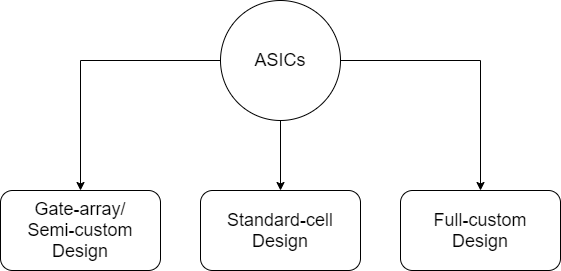
Figure 2 – Types of ASICs
As for the manufacturing of ASICs, there are three routes that can be chosen: standard-cell design, gate-array/semi-custom design and full-custom design. As we move from standard-cell design and move up to a fully customized design, the material costs and time required to create and then manufacture an ASIC increase dramatically. This has to be taken into consideration before the start of the process and some of the factors that we need to look at is the commercial value of the final product, the actual requirements for the chip and whether the solution will be a definitive answer to a problem or not.
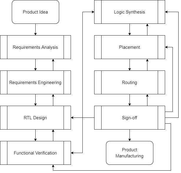
Figure 3 – Design Flow for Standard-cell design ASICs
Standard-cell designs use HDLs (Hardware Description Languages such as Verilog and VHDL) to describe the logic that is required and then, via a series of steps, the final ASIC is manufacturer.
The usual stages that go into making a standard-cell design ASIC are:
These steps form what is called ASIC design flow and by sticking to this, the final device will always be correctly implemented, unless flaws are introduced at the manufacturing foundry or in shipping.
As for gate-arrays and semi-custom design, it has certain benefits beyond the standard cells, but it comes at the cost of longer design and development cycles. The semi-custom approach is a compromise between quick design times and performance.
Today, gate-array ASICs are usually present in the form of structured ASICs that consist of a large CPU, digital signal processors, peripherals, standard interfaces, static RAM and a block of reconfigurable/programmable uncommitted logic.
Full-custom design is usually the most cost intensive ASIC development process, as the design must start from the semiconductor level and use HDLs to describe every layer of the ASIC. This approach is used by processor designers, like Intel, AMD and Nvidia, to create further optimized ASICs.
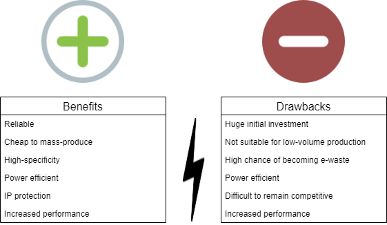
Figure 4 – ASIC advantages and disadvantages
Advantages that ASICs have over standard ICs are the reduced size, the better performance at lower power requirements, IP protection and lower manufacturing costs at large scales. But there are also the disadvantages, like the increased up-front cost of developing an ASIC and the increased difficulty in designing and testing, but these can be mitigated well by doing proper market analysis for the product that you have in mind before committing a large sum of funding to it.
Standard-cell ASICs are the cheapest of the three main types of ASICs and are usually an intermediary between semi-custom design ICs and fully-custom ICs. They have quick turnaround times, but lack the detail and precision of full-custom designed chips.
Semi-custom ASICs are a bit more expensive, but can have larger numbers of logic gates. Difficulties arise when it comes to routing, as some interconnects might require migration, which would increase the array needed, further driving up the cost. Also, these ICs can never use 100% of the available silicon wafer.
Full-custom ASICs are the most well-known and have big advantages and drawbacks. They can use less area (and therefore components cost less), offer higher performance and integrate other previously tested components, like microprocessor cores, forming a SoC. The disadvantages associated with this method of designing ASICs are the increased manufacturing and design times, increased engineering costs, added complexity on the CAD (Computer-Assisted Design) and EDA (Electronic Design Automation) systems, requiring a more qualified and experienced team of designers and engineers.
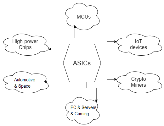
Figure 5 – ASIC use cases
Seeing as there is a lot of variety in how you can make an ASIC, you need to be able to choose the best technology to power your project or product.
For a low-volume production series or prototypes, ASICs are not economically viable, as the engineering costs are extremely high. Therefore, ASICs are recommended for high-volume production series, where the costs can be dampened across many devices.
Another application that is well-suited for ASICs is making an existing device smaller and/or more energy efficient and/or more performant. This is the reason why devices are constantly getting smaller, as ASICs penetrate the market further and further and drive the miniaturization of all devices, from the chips that provide the functionality of your car and phone, to the chips that power your fridge or automated coffee maker.
If you are worried about some other company or individual stealing your design, ASICs are a great way to ensure your design stays secret forever, as the actual design of ASICs prevents the theft of IP. It is very difficult to reverse engineer an Intel processor, for example. Thus, despite being on the market for over 50 years, no one has managed to figure out how to create an exact copy of their design.


