

An ASIC stands for Application Specific Integrated Circuit and is often assumed to be exorbitantly expensive to design and manufacture one. The reasons behind such a conjecture is are not entirely unfounded, given the fact that mask-set for the state-of-art semiconductor technology like 5nm costs around $10-15 million! This puts off many design companies towards making a decision to switch to an ASIC. However, there’s a catch.
One reason why lower technology nodes are more expensive is the increasing mask count. 130nm technology had around 30 masks, while the latest state-of-art 7nm technology uses around 70 masks. Mask costs alone can drive the project costs to a few million dollars. Add to it the Research and Development costs, equipment cost and material cost etc.
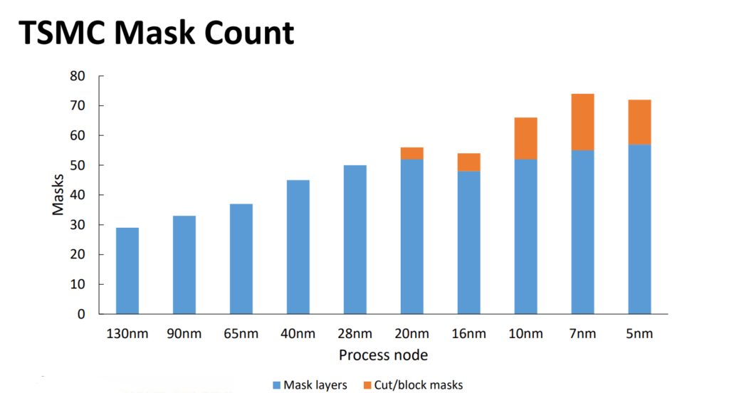
Figure 1: Increasing mask counts for advanced semiconductor technology. Source: IC Knowledge LLC
Top semiconductor manufacturers like Samsung and Intel are always ahead of the game when it comes to their semiconductor technology. This is pretty much also true for other fabless companies like Apple and Google, who are among first to migrate to a new technology. That’s because these companies design high-end CPUs for smartphones, servers or GPUs for performing matrix multiplications which are the heart of many artificial intelligence, machine learning and scientific algorithms which demand the best Power, Performance and Area metrics.
Fig. 2 shows the rising wafer cost as the process node is shrinking. The cost has increased up to 6 times from 130nm process node to the 7nm process node. This, however, comes at higher integration density where designers are able to put more devices in a given area.
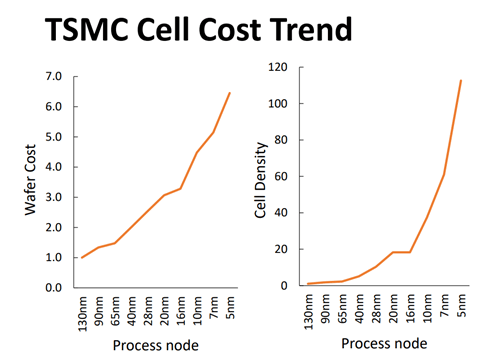
Figure 2: Wafer Cost for a process technology node. Source: IC Knowledge LLP.
IoT (Internet of Things) semiconductor market has been growing steadily over the last decade with the estimated sales projected to reach $30 billion by the end of 2019. Very seldom does IoT applications entail employing the best available semiconductor technology. Since IoT applications rely strongly on their interface with the real world, the IoT ASICs have a lot of analog circuitry. Analog circuitry demands high reliability and therefore IoT applications usually need a more mature technology which would not only be more reliable but would also bring the tool cost down.
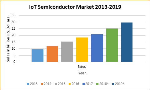
Figure 3: Growing IoT semiconductor market worldwide. Source: Statista 2018
Fig. 4 shows the drop in the nominal supply voltages as process technology node has shrunk. For 250nm technology, which began its production in the last 90s, the nominal supply voltage was around 2.5 Volts. By the time industry moved to 14nm in 2014, the nominal supply voltage has decreased to around 0.7 Volts. Analog circuits is particularly susceptible to the signal integrity, which decreases as the supply voltage decreases. This means, in addition to being cheaper, mature process technology nodes are most suitable for IoT applications which tend to have a lot of analog circuitry. This is especially true for IoT applications in the space of Connected Health for implanted medical devices such as the pacemaker, where reliability and accuracy are of paramount significance.
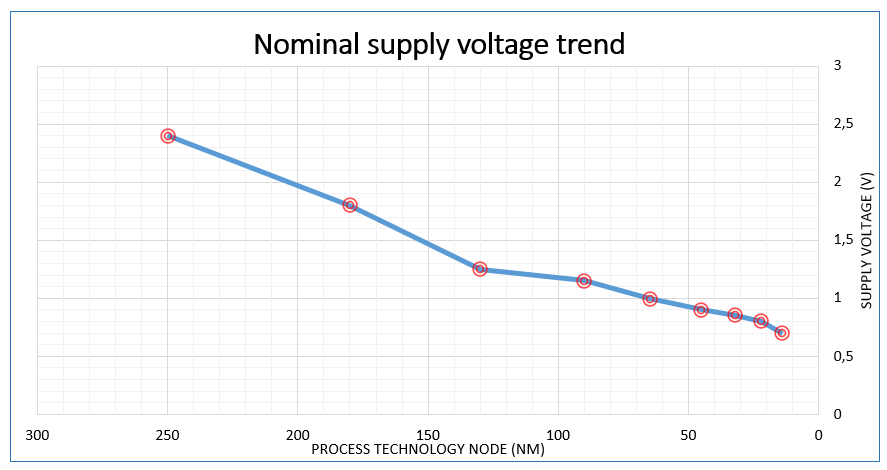
Figure 4: Nominal supply voltage drops rapidly as the process technology node shrinks
An IoT ASIC may comprise of many functional blocks. These blocks can be sub-divided into 4 major types:
With a PCB based solution, you would typically have separate ICs for most of these components connected together by wires. The ASIC implementation is capable of incorporating the same functionality on the same die, hence offering an elegant solution with smaller area and higher performance.
This is primarily because an ASIC can achieve higher packing density, with more transistors per unit area, and shorter interconnect lengths. An FPGA design can be up to 30 times bigger as compared to an ASIC design.
In addition to discarding the redundant circuitry, ASIC design also opens up new avenues for power management strategies like Power Domain separation, Dynamic Voltage Scaling (DVS), Dynamic Frequency Scaling (DFS) etc. On the other hand, one can only attempt the good old Clock Gating or perhaps Clock Domain separation on an FPGA.
For IoT applications like the Smart Home, Wearable Electronics and Connected Health, low power devices would be particularly appealing. Some estimates show that an FPGA may consume 9-12 times the amount of power as an ASIC
Product Cost = NRE + (P * RE)
NRE = Non Recurring Engineering Cost
RE = Recurring Engineering Cost per part
P = Total number of parts
While NRE cost (function of EDA Tools, Design for Test, Simulation, Masks etc.) is pretty much non-existent for an FPGA design, the RE cost (Function of wafer cost, production yield, packaging etc.) per part is higher. For higher volume of units manufactured, an ASIC would be far more economical than the FPGAs. It might be necessary to perform an analysis to find the break-even point to come up with the minimum number of parts needed that would make ASIC design cost at par with the FPGA design.
While we talked about all the advantages that ASIC can offer, let’s be realistic here. Our goal is not to entice anyone into making a decision in favor of an ASIC, rather to help choose an ASIC if it meets all the design and financial constraints while achieving smaller area, lower power, higher performance and lower cost. Before we conclude, it would be prudent to highlight the areas where an FPGA scores over an ASIC.
Perhaps the biggest advantage of choosing an FPGA lies with shorter time to market. An FPGA would be the answer to your needs to enter the market quickly with a working prototype. Getting a prototype working on FPGA might take a few months, however, an ASIC design might take up to 2 years, especially if you don’t really have a stable design methodology. Another advantage of FPGA is that it is configurable. It’s extremely easy and inexpensive to reprogram an FPGA with a new bit-stream, while it might take a few months to do the same on an ASIC, in addition to the high costs involved.
It would make complete sense to start off with an FPGA prototype and once proven, you can switch over to an ASIC for mass production to reap all the benefits mentioned above.
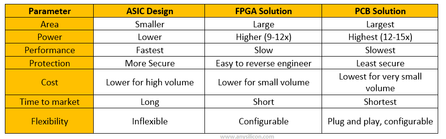
Figure 5: Comparing ASIC vs. FPGA vs. PCB Solution
To conclude, ASIC is the natural choice if you are looking for mass production of your design and interested in squeezing out every bit of performance, meeting an aggressive power budget while keeping the cost and size of your part relatively low. However, FPGA would be your best option if you are looking to hit the market early or you wish to showcase your prototype before entering mass production. We encourage you to contact ASIC design companies to do a feasibility analysis to determine the best solution for your design needs.


