That has made chiplets, HBM, silicon interposers, redistribution layers, bridges and 3D stacking increasingly important. Understanding the difference between 2.5D and 3D packaging is therefore becoming essential for ASIC and SoC architects, packaging engineers and companies planning next-generation semiconductor products.
2.5D vs 3D Packaging — Quick Comparison
| Feature |
2.5D Packaging |
3D Packaging |
| Die arrangement |
Dies are placed primarily side-by-side |
Dies are stacked vertically |
| Main interconnect structure |
Silicon interposer, RDL interposer or silicon bridge |
TSVs, microbumps, copper pillars or hybrid bonding |
| Typical examples |
GPU/AI accelerator + HBM |
HBM stack, 3D cache, stacked logic |
| Routing density |
Very high |
Extremely high |
| Thermal complexity |
High |
Higher because active dies may sit above one another |
| Manufacturing maturity in 2026 |
Very high for advanced AI/HPC production |
Growing rapidly; still more selective by application |
| Best fit |
Large multi-chiplet and HBM systems |
Maximum density, short interconnects and vertical integration |
What Is 2.5D Packaging?
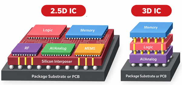
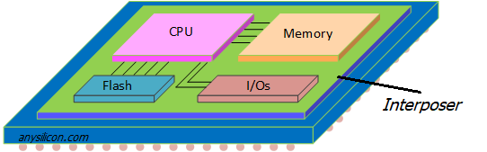
In 2.5D packaging, multiple dies are mounted next to each other on a high-density routing structure. That routing structure is typically a silicon interposer, an organic/RDL interposer, or a package substrate containing embedded silicon bridges.
The dies are not simply placed on an ordinary package substrate. The interposer provides much finer metal lines and much higher interconnect density than a conventional PCB or standard package substrate can support. This allows thousands of die-to-die signals to travel only a few millimeters between chiplets.
A typical 2.5D AI package may contain:
- one or more compute dies;
- several HBM stacks;
- I/O chiplets;
- a silicon or RDL interposer;
- a package substrate;
- power-delivery and passive components.
The term “2.5D” is not mathematically literal. It refers to the fact that the active dies are mostly arranged beside one another, while the interposer introduces an additional vertical level between the dies and the package substrate.
Why 2.5D Packaging Became So Important
The two most important motivations for advanced packaging are bandwidth and power.
At PCB level, routing density is limited by relatively coarse line-and-space rules. Additional PCB layers can add more routing, but traces become longer, signal integrity becomes harder to manage and cost rises.
Inside an advanced package, dimensions can be dramatically smaller. More signals can therefore run in parallel, and those signals travel over much shorter distances.
This is one of the fundamental reasons HBM is so effective. Rather than communicating with memory over relatively narrow board-level interfaces, the processor can connect to HBM through extremely wide buses inside the package.
More Bandwidth Without Simply Increasing Signaling Speed
There are two basic ways to increase the bandwidth between two semiconductor devices:
- increase the amount of data transmitted by each signal; or
- increase the number of signals operating in parallel.
High-speed electrical standards such as PAM4 increase data rate per lane, but signal-integrity challenges become increasingly difficult as frequency rises. Advanced packaging provides another path: use a much wider interface containing far more wires.
That is much easier when the processor and memory sit millimeters apart inside the same package instead of centimeters apart on a PCB.
Shorter Connections Can Reduce Power
Longer electrical connections generally require stronger drivers and greater signaling energy. Moving high-bandwidth communication into the package shortens the transmission path and can reduce energy per bit.
The total power of a system may still rise if the number of connections grows substantially, but the energy required for each individual connection can fall. This is a major reason chiplet designers try to keep high-bandwidth interfaces local to the package.
What Is 3D Packaging?
3D packaging stacks semiconductor dies vertically rather than placing all active dies next to each other. The dies communicate through vertical interconnect structures such as through-silicon vias (TSVs), microbumps, copper pillars or increasingly fine-pitch hybrid bonds.
The most familiar commercial example is high-bandwidth memory. HBM consists of multiple DRAM dies stacked vertically. TSVs run through the stack, allowing the memory dies to communicate with a base die and ultimately with the processor.
3D stacking can also be used for logic. A cache die can be placed on top of a compute die, or one logic chiplet can be bonded directly to another logic die.
Why Stack Dies?
Vertical stacking offers several important advantages:
- shorter die-to-die connections;
- higher interconnect density;
- smaller package footprint;
- potentially lower communication energy;
- more silicon functionality in the same package area;
- the ability to combine dies manufactured on different process technologies.
But stacking active dies creates new thermal, mechanical and testing challenges. Those tradeoffs explain why 3D packaging does not simply replace 2.5D packaging.
2D, 2.5D, 3D and 3.5D Explained
| Architecture |
Basic Arrangement |
Typical Use |
| 2D |
Die mounted directly on package substrate |
Conventional single-die and multi-die packages |
| 2.5D |
Multiple dies mounted side-by-side on an interposer or connected through bridges |
GPU/AI accelerator + HBM, HPC chiplets |
| 3D |
Dies stacked vertically |
HBM, stacked cache, logic-on-logic |
| 3.5D |
3D-stacked components combined with 2.5D integration |
Advanced AI/HPC packages with stacked logic plus multiple HBM stacks |
The distinction is useful, but real-world systems increasingly blur the boundaries. A package can contain vertically stacked HBM, side-by-side compute chiplets and local bridge connections at the same time.
That is why “3.5D” is often used informally to describe packages combining 3D stacks with a broader 2.5D architecture.
HBM Is Both 3D and Part of a 2.5D System
HBM provides a good example of why terminology can become confusing.
The HBM device itself is a 3D structure: multiple memory dies are physically stacked and communicate vertically through TSVs and fine-pitch interconnects.
However, an AI accelerator and its HBM stacks are commonly integrated using a 2.5D architecture. The processor and the HBM stacks sit beside each other on a silicon or RDL interposer.
So one package may simultaneously contain:
- 3D memory stacks;
- 2.5D processor-to-memory integration;
- multiple logic chiplets;
- a package substrate;
- potentially local silicon bridges or interconnect chips.
The Role of the Interposer in 2.5D Packaging
The interposer is one of the defining elements of traditional 2.5D packaging.
It forms another level in the connectivity hierarchy:
Die → Interposer → Package Substrate → PCB
Each level uses progressively coarser wiring. On-die metal is extremely dense, interposer routing is less dense but still much finer than package-substrate routing, and the PCB has the coarsest geometry.
This hierarchy makes it possible to keep massive die-to-die interfaces inside the package without exposing thousands of individual signals to the PCB.
Silicon Interposer
Silicon interposers provide the highest mature routing density because they are fabricated using semiconductor-style processing. They are widely used for very high-bandwidth HBM and chiplet integration.
Organic / RDL Interposer
RDL and organic interposers can reduce cost and support larger package areas, although they normally offer coarser geometry than silicon.
Silicon Bridge
A silicon bridge uses a small piece of silicon only where very high-density die-to-die routing is necessary. This can reduce the amount of expensive silicon used compared with a full-size interposer.
Intel’s EMIB is one of the best-known examples of this architecture.
How 3D Dies Are Connected
Several interconnect technologies are used as packages move from traditional assembly toward increasingly dense vertical integration.
| Interconnect |
Typical Role |
Relative Density |
Main Consideration |
| Wire bond |
Traditional die-to-package or low-cost stacked die |
Low |
Economical but limited I/O density and bandwidth |
| C4 / solder bump |
Flip-chip die attachment |
Medium |
Mature and economical |
| Microbump |
Fine-pitch die stacking and interposer connections |
High |
Pitch and underfill limitations become important |
| Copper pillar |
Fine-pitch controlled-height interconnect |
High |
Improved control of pitch and stand-off height |
| Hybrid bonding |
Very fine-pitch die-to-die or wafer-to-wafer stacking |
Very high |
Requires extremely flat, clean and precisely aligned surfaces |
Hybrid Bonding Changes the 3D Packaging Equation
Hybrid bonding is one of the most important technologies behind the next generation of 3D integration.
Unlike solder-based interconnects, hybrid bonding connects metal pads directly while also bonding the surrounding dielectric surfaces. Eliminating solder allows much smaller connection pitch and potentially lower electrical resistance.
This can make die-to-die links shorter, denser and more power-efficient than conventional microbumps.
The difficulty is manufacturing. The surfaces must be exceptionally clean and flat, alignment accuracy becomes critical, and every bonded die needs to have very high quality because replacing a defective die after bonding can be difficult or impossible.
2.5D vs 3D: Performance and Bandwidth
| Performance Factor |
2.5D |
3D |
| Die-to-die distance |
Short |
Extremely short |
| Interconnect density |
Very high |
Potentially highest |
| HBM integration |
Excellent |
HBM itself uses 3D stacking; system integration often remains 2.5D |
| Signal latency |
Low |
Potentially lower |
| Energy per bit |
Low compared with board-level communication |
Potentially lower still |
| Package footprint |
Larger than equivalent vertical stack |
Smaller footprint possible |
Thermal Challenges: The Major 3D Tradeoff
The biggest advantage of 3D stacking — placing dies extremely close together — can also become one of its largest engineering problems.
Every active die generates heat. In a side-by-side 2.5D layout, designers can often place high-power dies apart from heat-sensitive components and provide more direct heat-removal paths.
In a 3D architecture, one active die may sit directly above another. Heat generated by the lower die must travel through or around the upper die, while the upper die may also generate significant heat of its own.
This can produce:
- localized hot spots;
- higher junction temperatures;
- reduced allowable clock frequency;
- thermal gradients across the stack;
- increased thermomechanical stress;
- additional cooling requirements.
Advanced-package design therefore requires thermal analysis at the package level, not simply thermal analysis of each die in isolation.
HBM Creates a Special Thermal Challenge
HBM needs to sit close to the compute die because shorter connections improve bandwidth and power efficiency. But DRAM is sensitive to temperature, while the adjacent processor may be one of the hottest components in the system.
Packaging engineers therefore face a direct tradeoff: the memory should be electrically close to the processor but thermally isolated enough to operate reliably.
Reliability Challenges in 2.5D and 3D Packages
Advanced packages contain more materials, more interfaces and more interconnects than traditional packages. Three reliability issues become particularly important:
- co-planarity and warpage;
- electromigration;
- thermomechanical stress caused by CTE mismatch.
If a die, interposer or substrate is not sufficiently flat, some solder joints may form poorly. Those marginal joints may pass initial test but fail after mechanical shock or repeated thermal cycling.
Fine-pitch wiring also increases current density, making electromigration increasingly important. Engineers must analyze current flow not only inside the silicon but also across RDLs, interposers, bumps and other package structures.
Finally, silicon, organic substrates, solder and other package materials expand at different rates as temperature changes. Repeated thermal cycling can stress connections and eventually produce cracks or delamination if the package is not designed correctly.
Testing Becomes More Difficult as the Package Becomes More Integrated
Testing a multi-die package follows the same basic principle as testing an ordinary IC: engineers must be able to control internal nodes and observe the resulting behavior.
But multi-die systems make access more difficult. Once several chiplets are connected through an interposer or stacked vertically, some internal interfaces are no longer directly accessible through package pins.
Advanced-package test strategies therefore rely on technologies including:
- IEEE 1149.1 JTAG;
- IEEE 1149.6 for AC-coupled interfaces;
- IEEE 1687 / IJTAG for internal test infrastructure;
- BIST and MBIST;
- IEEE 1838 for stacked-die test access.
IEEE 1838 is particularly relevant to 3D integration because it defines mechanisms for accessing multiple test controllers in stacked dies, including cases where upper dies are accessible only through a lower die.
Known-Good Die Becomes More Important
A defective monolithic chip wastes one die. A defective chiplet inside an expensive multi-die package can waste the package, the interposer, HBM and every other die already assembled with it.
This makes known-good-die testing increasingly important as package value rises.
Testing must therefore occur at several stages:
- before die assembly;
- during intermediate package construction where possible;
- after final assembly;
- sometimes again at system level.
The economics of 3D packaging make this especially important because vertically bonded dies can be difficult to separate after assembly.
2.5D vs 3D Packaging Cost
There is no universal rule that 2.5D is inexpensive and 3D is expensive. Cost depends on the interposer material, die size, yield, interconnect pitch, assembly flow, test strategy, package size and production volume.
However, several general patterns apply.
| Cost Driver |
2.5D Impact |
3D Impact |
| Interposer |
Can be a major cost, especially large silicon interposers |
May still be needed if the 3D stack is integrated into a broader 2.5D package |
| Bonding |
Flip-chip and microbump processes are relatively mature |
Fine-pitch TCB or hybrid bonding can increase process complexity |
| Yield loss |
Failure can waste several dies plus interposer/package |
Stacking can multiply the financial impact of a defective die |
| Thermal design |
Complex but generally easier to spread heat laterally |
Often more demanding because of vertically stacked heat sources |
| Test |
Complex multi-chip test flow |
Even greater emphasis on known-good die and stacked-die access |
2026 Update: AI Is Pushing 2.5D Packaging Beyond Traditional Limits
AI demand is currently one of the biggest forces shaping advanced packaging.
TSMC describes CoWoS as a 2.5D platform for integrating multiple SoCs and HBM stacks for HPC and AI. Its CoWoS-S architecture supports silicon interposers up to roughly 3.3 times reticle size, or around 2,700 mm², while TSMC recommends CoWoS-L or CoWoS-R when package requirements move beyond that scale.
That size pressure is becoming increasingly important. TrendForce reported in September 2026 that AI chip packages are continuing to grow as suppliers add more compute dies and more HBM. The firm expects CoWoS-L to remain a mainstream advanced-packaging option through 2028, while Intel’s EMIB-T provides another path for connecting very large multi-die systems without relying on one enormous silicon interposer.
This means the next stage of 2.5D packaging is not simply about making today’s interposers larger. It is increasingly about combining RDL structures, local silicon bridges and new package architectures to move beyond reticle and wafer-area constraints.
2026 Update: 3D Packaging Is Moving Toward Hybrid Bonding
The major shift in 3D packaging is the move from solder-based microbumps toward much finer hybrid-bonded connections.
TSMC’s SoIC platform provides direct 3D chip stacking with sub-10 µm bond-pitch capability. TSMC says its 3 nm SoIC chip-stacking technology entered volume production in 2025 and positions the technology for high-density HPC integration.
Intel Foundry is pursuing a similar direction with Foveros Direct 3D. Intel’s current technology brief describes Foveros Direct 3D as true vertical die stacking using hybrid bonding, complementing its 2.5D EMIB and Foveros technologies.
Intel also describes its broader packaging roadmap as a continuum rather than a choice between 2.5D and 3D. EMIB provides side-by-side die integration, while Foveros Direct 3D provides vertical integration. These technologies can then be combined for more complex systems.
UCIe Is Expanding From 2.5D Toward 3D Chiplet Integration
Standardized die-to-die communication is another important piece of the 3D packaging roadmap.
The UCIe 2.0 specification adds explicit support for 3D packaging. UCIe describes UCIe-3D as being optimized for hybrid bonding, with support spanning bump pitches from approximately 10–25 µm down to around 1 µm or below.
This matters because one of the long-term goals of the chiplet ecosystem is interoperability: a system designer should eventually be able to combine dies from different suppliers using standardized physical and protocol interfaces.
3D packaging makes that challenge more difficult because pitch, testability, thermal design and mechanical assembly all become more tightly coupled.
2.5D vs 3D: Which Should You Choose?
Choose 2.5D When:
- You need to integrate one or more compute dies with several HBM stacks.
- The package requires very high die-to-die bandwidth but vertical stacking is unnecessary.
- You want a mature, production-proven architecture.
- Thermal separation between high-power components is important.
- Different chiplets need to sit side-by-side across a large package area.
- A silicon bridge or RDL architecture can reduce full-interposer cost.
Choose 3D When:
- Package area is severely constrained.
- The shortest possible die-to-die links are important.
- Interconnect density must exceed practical 2.5D routing density.
- A cache, memory or logic layer naturally benefits from vertical placement.
- The design can support the required thermal-management strategy.
- The project has access to suitable hybrid-bonding or fine-pitch stacking technology.
Choose a Combined 3.5D Architecture When:
- You need vertically stacked logic or memory together with HBM.
- The system includes many different chiplets.
- Some interfaces need 3D-level density while others need large-area 2.5D routing.
- You are designing a next-generation AI/HPC package where both bandwidth and total silicon area are extremely large.
Application Examples
| Application |
Likely Packaging Direction |
Why |
| AI accelerator with multiple HBM stacks |
2.5D |
Wide processor-to-HBM interfaces and mature production ecosystem |
| HBM stack itself |
3D |
DRAM dies are vertically stacked and connected through TSV-based structures |
| Stacked cache on processor |
3D |
Very short processor-to-cache interconnect and package-area savings |
| Large multi-chiplet HPC processor |
2.5D / bridge-based |
Side-by-side chiplets can occupy a large package area |
| Future stacked logic + HBM AI system |
3.5D |
Combines vertical logic integration with broad 2.5D HBM connectivity |
| Cost-sensitive chiplet SoC |
2.5D RDL / local bridge |
Dense silicon routing can be limited to the regions where it adds value |
Advanced Packaging Requires Chip-Package Co-Design
Traditional semiconductor development often treated packaging as a downstream activity. The chip was designed first and then handed to packaging engineers.
That model becomes increasingly difficult with 2.5D and 3D systems.
The package now directly affects:
- signal integrity;
- power integrity;
- chiplet placement;
- HBM placement;
- clock frequency;
- thermal performance;
- mechanical stress;
- interconnect latency;
- testability;
- system cost.
For chiplets arranged side-by-side, interposer parasitics influence system performance and power. For stacked dies, thermal behavior and vertical interconnect resistance become part of the architecture itself.
That means chip, interposer, package, thermal and test teams need to collaborate from the planning stage rather than waiting until silicon design is finished.
What Engineers Should Define Before Selecting 2.5D or 3D
| Requirement |
Question to Answer |
| Bandwidth |
How many Tb/s or die-to-die lanes are required between chiplets and memory? |
| Package size |
Can all required dies fit side-by-side, or must some be stacked? |
| Thermal budget |
Can the cooling system handle stacked active dies? |
| Interconnect pitch |
Are microbumps sufficient, or is hybrid bonding required? |
| Yield |
How will known-good die be verified before assembly? |
| Test access |
Can each die and internal interface be controlled and observed? |
| Cost |
Does the system need a full silicon interposer, an RDL interposer, or local silicon bridges? |
| Reliability |
What warpage, CTE, electromigration and thermal-cycle requirements apply? |
| Manufacturing partner |
Which foundry or OSAT has a qualified process for the required architecture? |
Final Takeaway
2.5D and 3D packaging are complementary rather than competing technologies. 2.5D is currently the workhorse for AI processors, HPC chiplets and HBM because it combines extremely high bandwidth with mature high-volume manufacturing. 3D packaging pushes integration density further by stacking dies vertically, shortening die-to-die connections and enabling architectures that cannot fit efficiently in two dimensions.
In 2026, the clearest industry direction is toward combining them. Large AI systems increasingly need both horizontal scale — many compute dies and HBM stacks across a large package — and vertical density — stacked memory, cache or logic connected through finer-pitch bonding.
The result is a packaging roadmap where the distinction between 2.5D and 3D becomes less important than the system-level question: which components should sit beside each other, which should be stacked, and which interconnect technology delivers the required bandwidth, power, thermal performance, yield and cost?
Need a 2.5D, 3D or Advanced Packaging Partner?
AnySilicon can help semiconductor companies connect with packaging, substrate, interposer, chiplet assembly and test providers for BGA, flip-chip, HBM, 2.5D, 3D and other advanced-package projects.
Submit Your Packaging Requirement →
Related AnySilicon resources: Silicon vs Organic vs Glass Interposers, BGA Packaging Services, and BGA Substrate Design.
Sources and Further Reading
- Semiconductor Engineering, Advanced Packaging Fundamentals (2025) — primary technical foundation for 2.5D/3D architecture, HBM, interposers, TSVs, bonding, thermal design, test and reliability.
- TSMC 3DFabric – CoWoS — current 2.5D production platforms, interposer scaling and AI/HPC positioning.
- TSMC 3DFabric – SoIC — current 3D chip-stacking technology and volume-production information.
- Intel Foundry – Foveros Direct 3D Technology Brief — Intel’s current 2.5D, 3.5D and direct 3D packaging roadmap.
- UCIe Consortium – Specifications — UCIe 2.0 support for 3D packaging and hybrid-bonded chiplets.
- TrendForce, September 2026 – AI packaging beyond reticle limits — 2026 market update covering CoWoS-L, EMIB-T, package growth and AI/HBM demand.