

Imagine a world where data moves at the speed of light—literally. Silicon photonics makes this possible, merging optics with the familiar silicon used in traditional electronics.
This advanced technology, originating from the 1980s, stands today as a pivotal innovation in microelectronics. It offers faster data transfer rates and lower power consumption compared to electronic-only systems.
As we delve into the intricate world of ASIC design for silicon photonics, we’ll explore the key components, integration strategies, design challenges, and the myriad of applications that stand to revolutionize how we process and transmit information in the digital age.
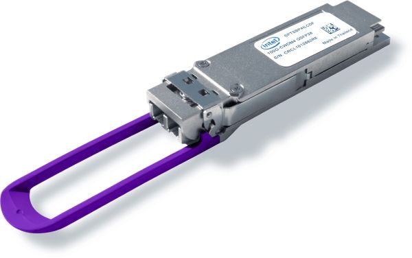
(Credit: Intel Corporation)
Silicon photonics is a transformative technology that merges the advantages of photonics and semiconductor electronics on a single platform. At its core, silicon photonics involves the use of silicon as a medium for transmitting and manipulating light signals, essentially enabling optical communications within silicon chips. The integration of photonics with silicon-based electronics revolutionizes data communication, allowing for faster, more efficient transfer of large volumes of data compared to traditional electronic devices.
The concept hinges on the interaction between photons—particles of light—and electrons within the silicon substrate. Silicon, the cornerstone of contemporary electronics, is characterized by its cost-effectiveness, high-performance capability, and a mature manufacturing ecosystem. By leveraging the existing silicon infrastructures, silicon photonics brings forth a synergy of electronic and optical functions that promises to overcome bottlenecks in speed and bandwidth faced by purely electronic systems.
Furthermore, this merger significantly expands the functional capabilities of application-specific integrated circuits (ASICs). ASICs are tailored for particular uses rather than general-purpose applications, offering optimized performance and power usage for targeted tasks. By integrating silicon photonics, ASIC designs can achieve unprecedented levels of functionality, such as high-speed optical data links, that were once considered unattainable using traditional silicon electronics alone.

Silicon photonics can be defined as the study and application of photonic systems which use silicon as an optical medium. The term encompasses a broad range of technologies aimed at routing, modulating, generating, and detecting light on silicon-based integrated circuits. A typical silicon photonic device comprises an array of optical components, such as waveguides, modulators, and detectors, all fabricated using semiconductor processing techniques similar to those used for electronic integrated circuits.
A key attribute that makes silicon an excellent platform for photonics is its transparency in the near-infrared communication bandwidth, particularly around the 1.55-micrometer wavelength used in fiber optic telecommunications. Additionally, silicon’s high refractive index allows tight light confinement and compact photonic devices, making it ideal for densely integrated photonic circuits.
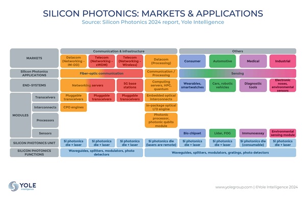
Data centers are the primary application for silicon photonics, with new Chinese leaders emerging daily. Telecommunications is another key area that leverages silicon’s superior performance. Optical LiDAR systems also show promise but face cost and beam-scanning hurdles.
The evolution of silicon photonics began in the latter part of the 20th century as researchers sought to exploit silicon’s potential beyond its established role in electronics. Progress in the field was initially gradual, constrained by silicon’s indirect bandgap, which rendered it inefficient as a light source. Nevertheless, advancements in epitaxial growth and wafer bonding technologies enabled the integration of other materials, like III-V compounds, with silicon to incorporate active components such as lasers.
In the following decades, significant research efforts were dedicated to overcoming the challenges of silicon as an optical medium, leading to a surge in the development of advanced photonic devices. The emergence of silicon nitride (SiN) as a complementary material further bolstered the growth of the field, offering low-loss waveguides and facilitating broader wavelengths of operation.
The industry experienced a paradigm shift with the introduction of process design kits (PDKs), which formalized the methodologies for silicon photonic circuit design. This standardization, alongside continual breakthroughs in heterogeneous and 3D integration techniques, has substantially accelerated the commercial adoption of silicon photonics.
Incorporating silicon photonics within ASIC design yields several crucial advantages, offering a leap in performance and efficiency. Here are some of the key benefits:
These benefits solidify silicon photonics’ role as a pivotal technology for the future of ASIC design and underline its potential to revolutionize sectors reliant on high-speed data transfer, such as telecommunications, data centers, and high-performance computing.
The basic components in silicon photonics form the foundation for manipulating and guiding light through an integrated circuit. These components include, but are not limited to, optical waveguides, modulators, detectors, and multiplexers. The key to the functionality of these components lies in their ability to interact with light at the chip level. Waveguides, which are the optical equivalent of electrical wires, channel light signals with precision. Modulators play a crucial role in controlling the light signal, often by varying its intensity, phase, or polarization to encode data. Photodetectors convert these light signals back into electrical signals, allowing for information to be processed by electronic circuits. Additionally, multiplexers and demultiplexers are deployed to separate and combine light signals of different wavelengths, enabling efficient data transmission over a single optical fiber.
At the heart of silicon photonics lie photonic circuits, which are complex networks of photonic components integrated onto a silicon chip. The primary function of these circuits is to manipulate light signals for the purposes of data transmission, processing, and sensing. The building blocks of these circuits are optical waveguides, slender structures that guide light with minimal loss. Created using techniques like lithography and etching, these waveguides confine light via total internal reflection, akin to how fiber optics operate, but on a much smaller scale. The light is typically guided through the silicon layer or a silicon nitride layer, each providing different benefits in terms of loss and bandwidth.
Materials play a pivotal role in determining the performance of waveguides. Silicon, with its high refractive index, enables tight confinement of light and facilitates miniaturization. Silicon nitride, though having a lower refractive index, is used where lower propagation loss and broader wavelength operation are required. Advances in materials and fabrication continue to enhance the capabilities and applications of photonic circuits.
Silicon wafers form the base upon which silicon photonic devices are built. The purity and crystallographic quality of the silicon used directly influence the performance of the photonic components. Wafers are commonly doped with other elements to modify their electrical and optical properties, catering to the needs of specific photonic applications.
The integration of materials such as III-V compounds, which are materials combining elements from groups III and V of the periodic table, onto silicon wafers has been a significant leap forward. Such integration enables active components like lasers, which silicon itself cannot efficiently produce due to its indirect bandgap. Heterogeneous integration techniques have allowed for the combination of these disparate materials to create high-performance photonic devices on a silicon chip. Moreover, the advent of silicon nitride (SiN) within this domain has brought about devices with lower losses and a wider spectral range.
Silicon photonics transceivers represent a key application of the technology, converting electrical signals into optical signals, and vice versa, for high-speed data communication. A transceiver combines multiple photonic and electronic elements, including lasers, modulators, waveguides, and detectors, all integrated onto a single chip. This level of integration leads to smaller form factors, reduced power consumption, and enhanced performance compared to traditional optical components.
Other optical components crucial to the performance of silicon photonic systems include filters, which select specific wavelengths of light; splitters, which divide light into multiple paths; and couplers, which facilitate the transfer of light between waveguides and optical fibers. The use of grating couplers, which diffract light into and out of the waveguides, is common for coupling light efficiently. These components are indispensable for a myriad of applications ranging from telecommunication to biophotonic sensing.
Silicon photonics is a domain defined by its components, each playing a distinct role in manipulating light for faster, more efficient data processing and communication. Through meticulous design and integration, these components coalesce into sophisticated systems that push the boundaries of what’s possible with integrated photonics.
Silicon photonics brings a significant evolution to Application-Specific Integrated Circuit (ASIC) design by leveraging the unique advantages of optical communication within the architecture of integrated circuits. The synchronization of photonic components with electronic ASICs presents an innovative approach to circumvent limitations faced by electrical links, especially as link reach shrinks and data rates increase. Silicon photonics integrates with ASICs to create systems that benefit from the high bandwidth and low latency of optical signals while maintaining the processing power of electronic circuits. Key benefits include reduced power consumption, increased data bandwidth, and miniaturization, allowing for denser and more efficient ASICs.
Co-packaging silicon photonics with ASICs refers to the process of integrating both photonic and electronic components into a single package. This coalescence aims to minimize the distance between the optics and electronics, thereby reducing interconnect losses and power consumption. Co-packaged optics are particularly crucial as data centers move towards higher-speed interfaces and the need for efficient, high-speed interconnects becomes more pressing.
By bringing the light source closer to the ASIC, co-packaged silicon photonics diminishes reliance on high-power copper links, which are less efficient over long distances. The key features of co-packaged silicon photonics include integrated lasers, modulators, and detectors alongside the electronic circuits in a compact form factor. This enhances the overall system performance and enables more streamlined communication infrastructure.
Heterogeneous integration in silicon photonics refers to the strategic combination of different materials and components onto a single silicon substrate, thereby combining the best attributes of various technological platforms. It commonly involves integrating III-V materials such as indium phosphide or gallium arsenide, known for their direct bandgap properties, which are essential for creating efficient light sources like lasers on the fundamentally indirect bandgap silicon platform.
Hybrid integration expands on this concept by combining separately fabricated components into a single device. This approach allows for the creation of photonic devices that might be difficult or impossible to fabricate using a single material system. Here are the critical advantages:
Monolithic integration in silicon photonics is the process of fabricating all photonic components—waveguides, modulators, detectors—on the same silicon substrate, avoiding the use of different material systems. This leads to seamless integration, resulting in reduced interface losses, simplified alignment, and potentially lower production costs. The process typically relies on a well-established silicon manufacturing ecosystem and can utilize Process Design Kits (PDKs) to standardize the production of photonic circuits.
Seamless integration is the ultimate goal of monolithic integration, where the interfaces between different components are so well integrated that they function as a single, unified system. This approach is instrumental in improving reliability, scalability, and performance of silicon photonics systems. It streamlines the manufacturing process and is pivotal for realizing fully integrated photonic solutions that can be mass-produced for a wide range of applications.
The choice between heterogeneous, hybrid, and monolithic integration depends on the specific application requirements, trade-offs in performance and cost, and available fabrication technologies. These integration strategies reinforce the diverse and adaptable nature of silicon photonics in ASIC design.
Designing ASICs for silicon photonics involves navigating a unique set of challenges and crafting solutions that fulfill the stringent requirements of optical communications. One major hurdle lies in the realization of high-performance photonic circuits that must coexist with electronic counterparts on a single chip. Careful design considerations are needed to prevent crosstalk and maintain the integrity of optical signals amidst electronic noise.
Solutions often involve refining the layout and isolation techniques. Fabrication challenges also arise due to the intricacies of layering both electronic and photonic components accurately. Addressing these issues, a new generation of Process Design Kits (PDKs) specific to silicon photonics is being developed, to streamline design processes and realize reliable, reproducible integrated circuits.
In silicon photonics, achieving power efficiency is paramount. Optical transceivers consume a significant amount of power, a large portion of which is attributed to the laser source. Optimizing power consumption begins at the design stage, where waveguides and modulators should be engineered to operate with minimal losses.
Utilizing silicon nitride in waveguides can help as it offers low propagation loss. Moreover, incorporating co-packaged optics can also reduce power requirements by shortening the distance optical signals must travel. Active components, such as modulators and detectors, must be engineered to operate effectively at low power levels to further boost the overall efficiency of the silicon photonic ASIC.
Coupling light efficiently from external sources, such as fibers, into the on-chip waveguides is a critical step in silicon photonics that can be plagued by losses. Efficient coupling requires precise alignment and optimization of the waveguide’s geometry.
Innovative designs, like inverse tapers and grating couplers, have been developed to tackle such challenges. Inverse tapers allow for a gradually changing waveguide width, minimizing reflection and enhancing coupling efficiency. Grating couplers, on the other hand, diffract light into the waveguide from an off-chip source, allowing for more flexibility in alignment.
As we transition from copper links to optical fibers, new challenges emerge. While optical interconnects provide superior data transmission rates over longer distances without electromagnetic interference, they also require precise alignment and robust connections to function effectively.
Electrical interconnects still play a crucial role in providing power and enabling communication between different sections of the ASIC. A major challenge is maintaining signal integrity at high frequencies. Solutions include designing with minimized parasitic capacitance and inductance, as well as enhanced shielding techniques. These advancements ensure that the electronic portions of the ASIC can keep pace with the high-speed optical components.
Moving from prototyping to high-volume manufacturing presents an array of issues in silicon photonics. Uniformity, yield, and cost-effectiveness are critical factors for the adoption and success of photonic chips in the marketplace.
Advanced manufacturing processes such as deep ultraviolet (DUV) lithography are being applied to fabricate intricate photonic structures with high precision. Additionally, efforts toward standardized PDKs allow for replicable designs that cater to mass production. The integration of electronic and photonic elements on a single chip must be rigorously controlled to ensure each photonics chip maintains the high quality needed for commercial applications.
The integration of ASICs crafted for silicon photonics within various sectors is revolutionizing modern technologies. These application-specific integrated circuits pave the way for high-density, energy-efficient optical communications infrastructure. Below are some of the key applications and benefits:
In the realm of optical communications, silicon photonics-based ASICs facilitate the development of compact and power-efficient optical transceivers necessary for high-speed data transfer. Data centers stand as key beneficiaries, with the implementation of silicon photonics enabling low-latency and high-bandwidth connections that can address the increasing data traffic demands. Furthermore, co-packaged optics alongside ASICs contribute to reducing power consumption across vast networks, enhancing thermal management, and optimizing space within servers — integral as link reach shrinks and data centers become increasingly dense.
High-performance computing (HPC) systems and artificial intelligence (AI) platforms require rapid and efficient processing of colossal datasets. Silicon photonics enables high-speed interconnects that can bridge the data transmission gap, propelling the HPC and AI fields forward. With the use of integrated lasers and photonic circuits, these systems gain the ability to perform complex computations more swiftly, promoting breakthroughs in machine learning, neural network training, and scientific simulations.
Silicon photonics ASICs have a transformative impact on biomedical devices and sensing applications. By miniaturizing optical components onto a silicon chip, it becomes feasible to create non-invasive diagnostic tools with high sensitivity. Optical coherence tomography and biosensors are just two examples benefiting from silicon photonic technologies, allowing for real-time monitoring of biological parameters. Photonic devices can also be used in lab-on-a-chip systems, offering a compact and cost-effective solution for both point-of-care diagnostics and research.
Looking ahead, the potential applications of silicon photonics span several emerging and innovative territories. Autonomous vehicles may employ silicon photonic-based sensors for enhanced navigational accuracy. Augmented and virtual reality technologies could also see improvements in performance and form factor through photonic-based display and communication advancements. Additionally, the development of new materials, such as III-V materials for light sources, and innovative techniques like 3D and heterogeneous integration, indicate a future where integrated photonic systems could become ubiquitous in both consumer and specialized devices.


