

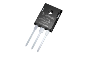
What is a TO-247 Package?
The TO-247 package is a widely used through-hole semiconductor package designed for high-power applications. It is commonly used for devices such as MOSFETs, IGBTs, diodes, and power transistors that require efficient heat dissipation and high current handling.
TO-247 stands for “Transistor Outline 247”, and
Looking for obsolete Xilinx IC chips?
We help you source discontinued Xilinx components or identify replacement solutions quickly. Get matched with verified global suppliers within 24–48 hours.
Why Xilinx Components Become Obsolete
Xilinx (now part of AMD) has released multiple generations of FPGA and programmable devices over

Looking for hard-to-find IC chips?
We help you locate rare, discontinued, and hard-to-source semiconductor components through a global network of verified suppliers. Submit your requirement and get matched within 24–48 hours.
Submit your requirement and get matched within 24–48 hours.
What Are Hard-to-Find IC Chips?
Read More

Looking for end-of-life (EOL) semiconductor components?
When components reach EOL, sourcing them becomes difficult and risky. We help you find available stock or identify replacement solutions quickly through a global network of verified suppliers.
Submit your requirement and get matched within 24–48 hours.
What Are
Need to replace an obsolete IC?
When a component is no longer available, finding the right replacement quickly is critical. We help you identify compatible alternatives or explore redesign and ASIC replacement options.
What Is an Obsolete IC Replacement?
An obsolete IC replacement refers to finding an
Struggling to find obsolete semiconductor chips?
Get matched with verified suppliers or explore replacement options fast. Submit Your IC Requirement.
Where to Buy Obsolete IC Chips
Obsolete IC chips are no longer available through authorized distributors, but they can still be sourced through alternative supply channels.
Read More