

In the fast-evolving landscape of semiconductor technology, the term “fabless semiconductor companies” stands as a testament to innovation and adaptability. These companies epitomize a strategic approach, focusing on design, innovation, and market agility while outsourcing the manufacturing aspect of semiconductor production. In this dynamic realm, giants like Qualcomm and Nvidia have made significant strides, crafting cutting-edge chips that power our devices.
Meanwhile, companies like Arm Holdings, known for their processor architecture, have revolutionized industries without owning fabrication facilities. These entities exemplify the prowess of fabless semiconductor companies, reshaping industries through ground-breaking designs and technological prowess.
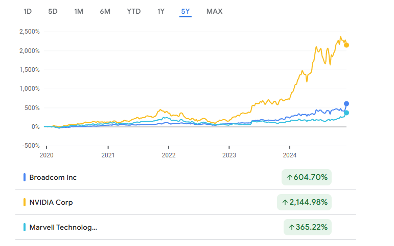
Figure 1: Broadcom, NVIDIA and Marvell’s Share Price Over the Last 5 Years
Fabless semiconductor companies are entities that specialize in the design, development, and marketing of semiconductor chips, while outsourcing the fabrication or manufacturing process to third-party foundries. These companies focus on innovation, creating chip designs, intellectual property (IP), and specifications for various electronic devices such as smartphones, computers, IoT devices, and more. Unlike integrated device manufacturers (IDMs) that handle both chip design and fabrication in-house, fabless companies leverage external foundries for the physical manufacturing of their semiconductor designs.
This business model allows fabless semiconductor companies to concentrate on innovation and design without the significant capital investment required for owning and operating fabrication facilities, enabling agility and competitiveness in the rapidly evolving semiconductor industry. Examples of fabless semiconductor companies include Qualcomm, Nvidia, Broadcom, MediaTek, and AMD.
New players entering the semiconductor market often opt for a fabless business model due to several compelling reasons:
Cost Efficiency: Building and operating a fabrication facility (fab) demands massive upfront capital investment. For new entrants, especially startups, this capital requirement can be prohibitive. Going fabless allows companies to channel resources primarily into research, development, and innovation rather than infrastructure.
Focus on Core Competencies: Semiconductor design and innovation are core strengths for many startups. By outsourcing fabrication, these companies can concentrate on honing their design capabilities, creating novel chip architectures, and optimizing performance rather than diverting resources to manage manufacturing complexities.
Technological Access: Accessing cutting-edge manufacturing technology is a significant challenge. Foundries investing in fabrication technology can provide smaller players access to advanced nodes that would otherwise be financially out of reach.
Flexibility and Scalability: Fabless models offer flexibility in adapting to market demands. Companies can scale production without being tied to the capacity limitations of in-house fabs. This agility allows faster responses to market changes and demand fluctuations.
Challenges associated with owning a fab, especially for new players, include:
High Upfront Costs: Building and maintaining a fab involves significant expenses like construction, equipment, and ongoing operational costs, which can overwhelm startups.
Tech Advancements: Semiconductor tech evolves rapidly. Keeping up requires continuous investment in equipment upgrades and newer manufacturing methods.
Scaling Challenges: Cost efficiency often needs high production volumes. Newcomers might struggle to achieve this scale, impacting their competitiveness.
Capacity Risks: Forecasting demand accurately is tough. Owning a fab means facing risks of overcapacity or underutilization, impacting efficiency.
Complex Operations: Fabs demand precise management, from quality control to supply chain intricacies and compliance. Navigating these complexities is tough for newcomers.
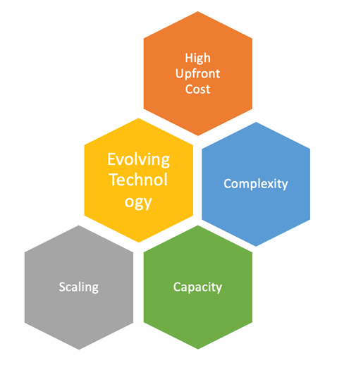
Figure 2: Challenges of Owning a Fab
By opting for a fabless model, new players can mitigate these challenges, focusing on their strengths in design and innovation while leveraging the expertise and infrastructure of specialized foundries to bring their semiconductor designs to market. There are two major fabless models to choose from, each offering a mixed bunch of pros and cons:
COT Model (Customer-Owned Tooling): Fabless companies in the COT model own or rent manufacturing tools, like mask sets, for semiconductor fabrication. This requires a significant upfront investment but offers greater customization and control over the manufacturing process. Long-term cost benefits can be realized by avoiding markups to external foundries.
ASIC Model (Application-Specific Integrated Circuit): Fabless companies in the ASIC model outsource semiconductor fabrication to external foundries. They pay for fabrication services based on production volume, with lower upfront costs and limited customization. However, this model provides access to diverse foundries and advanced technologies without the need for tool ownership.
In essence, the COT model involves ownership of manufacturing tools, allowing customization but requiring high initial investment, while the ASIC model outsources fabrication, offering flexibility and lower upfront costs but with limited control over the process. The choice depends on factors like customization needs, budget, and long-term cost considerations.
Starting a fabless semiconductor company involves several key steps. Here’s a comprehensive guide to all the steps and key points one need to evaluate before starting their fabless company:
Market Research and Expertise:
Business Plan Development:
Team Formation:
Intellectual Property Protection:
Work with legal experts to file for patents to protect your semiconductor designs, algorithms, and innovations. Implement robust measures to safeguard trade secrets and confidential information within your organization.
Partnerships and Supply Chain:
Funding Strategy:
Design and Development:
Testing and Validation:
Production and Quality:
Market Entry:
Starting a fabless semiconductor company demands a mix of technical expertise, business acumen, strategic planning, and adaptability. Executing each step meticulously while staying responsive to market shifts and technological advancements is key.
Selecting the right partners and tools is pivotal for the success of a fabless company. Following are the key considerations involved in choosing these critical entities:
Selecting the Ideal Foundry Partner:
Choosing the right foundry partner involves assessing various factors:
Technology Alignment: Leading foundries like TSMC (Taiwan Semiconductor Manufacturing Company), Samsung Foundry, and GlobalFoundries offer diverse process nodes catering to different chip design needs.
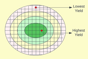
Quality and Yield: Foundries such as TSMC and Samsung Foundry have a proven track record of high-quality chip manufacturing and reliable yields, ensuring chip success and market competitiveness.
Support and Services: Foundries like TSMC and GlobalFoundries provide robust support services and collaboration, crucial for seamless chip manufacturing.
Read more: How to Choose a Process Node
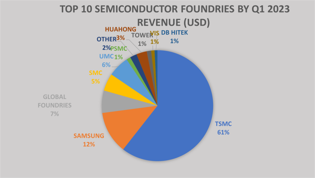
Figure 3: Revenue (in USD) of top 10 semiconductor foundries by Q1 2023
Identifying the Best Soft IP Vendor:
Selecting a soft IP vendor involves evaluating IP offerings and support:
IP Portfolio: Vendors like Synopsys, ARM, and Cadence Design Systems offer extensive libraries encompassing various IP cores, providing fabless companies with a wide range of functionalities.
Quality and Customization: Companies like ARM and Synopsys are known for their high-quality, customizable IP cores, allowing for differentiation in chip designs.
Support and Updates: ARM and Synopsys, among others, offer regular updates and strong support services, ensuring the reliability and compatibility of their IP cores.
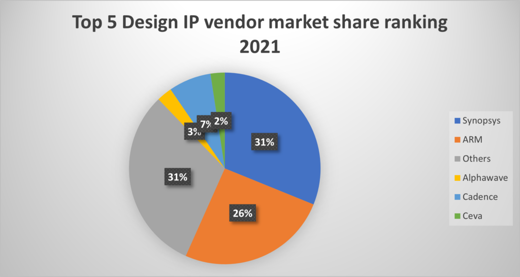
Figure 4: Market Share of top 5 design IP vendors
Choosing the Right EDA Tools:
The selection of Electronic Design Automation (EDA) tools significantly impacts chip design:
Tool Capabilities: Industry leaders like Synopsys, Cadence, and Mentor (a Siemens Business) offer comprehensive suites of EDA tools covering various design stages, ensuring efficiency and productivity.
Compatibility and Integration: Synopsys, Cadence, and Mentor provide tools that seamlessly integrate within the design flow, avoiding compatibility issues and streamlining the design process.
Support and Training: These vendors offer robust support, training, and user communities, empowering fabless companies to leverage their tools effectively.
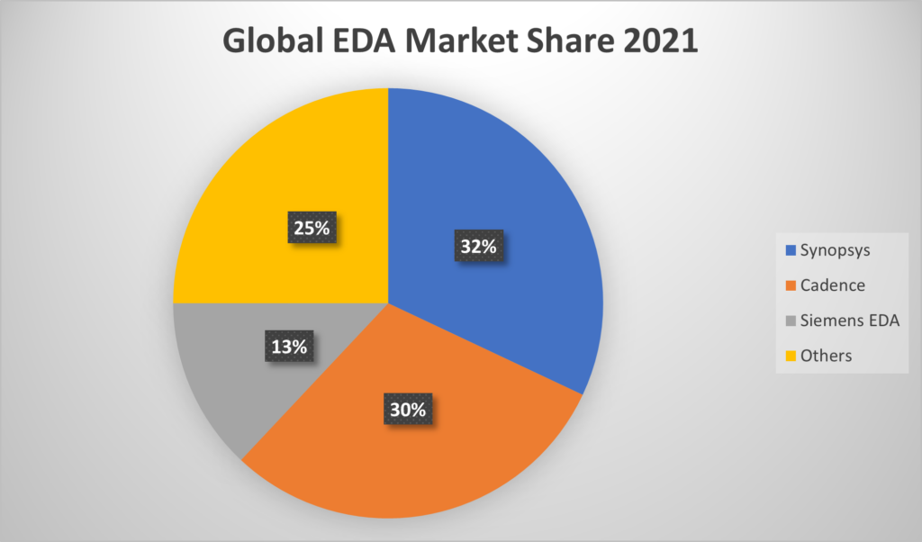
Figure 5: Global EDA Market Share 2021
Starting a fabless semiconductor company is a big challenge but also a chance to innovate. It’s not just about making chips, it’s about shaping the future of tech. Remember, teamwork and partnerships are key. Embrace challenges as opportunities to create something new. Stay flexible in a changing world and foster a culture of creativity. Your company isn’t just a business, it’s a story in the making, shaping the tech world ahead.
The follow section outlines the process for a fabless semiconductor startup, from initial specification to final product testing and cost estimation.
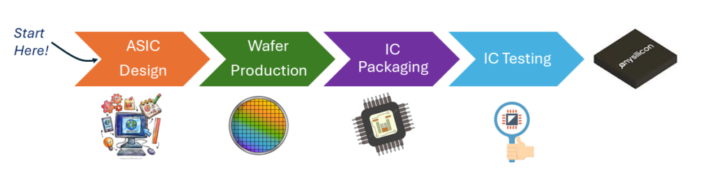
The process can be broadly divided into front-end and back-end design, followed by manufacturing and testing. A typical schedule might look like this (times are estimates and highly dependent on complexity):
Phase 1: Front-End Design (4-6 months)
Specification & Architecture Definition (1 month): Detailed definition of chip functionality, performance targets, power consumption, and interface requirements. This includes creating a system-level architecture diagram and defining key specifications.
RTL Design & Verification (2-3 months): Writing Register Transfer Level (RTL) code using a Hardware Description Language (HDL) like Verilog or VHDL. This involves extensive simulation and verification to ensure functionality and timing correctness. This phase often uses tools like ModelSim or QuestaSim.
Synthesis & Optimization (1 month): Translating the RTL code into a gate-level netlist, optimizing for area, power, and performance. Tools like Synopsys Design Compiler are commonly used.
Phase 2: Back-End Design (3-4 months)
Floorplanning & Placement (1 month): Arranging the logic blocks and I/O pads on the chip die. This is crucial for optimizing signal routing and minimizing delays. Tools like Cadence Innovus are often used.
Routing (1 month): Connecting the logic blocks and I/O pads using metal layers. This phase aims to minimize signal delays and ensure signal integrity.
Physical Verification (1 month): Comprehensive checks to ensure the design meets manufacturability rules (DRC/LVS) and timing constraints (STA). This involves tools like Calibre and PrimeTime.
Tapeout (1-2 weeks): The final step before manufacturing, where the design data is sent to the foundry.
Phase 3: Manufacturing & Testing (2-4 months)
Wafer Fabrication (Foundry): The foundry manufactures the wafers based on the tapeout data.
Wafer Testing: Initial testing of the wafers to identify defective dies.
Packaging: The working dies are packaged.
Final Testing: Comprehensive testing of the packaged chips to ensure functionality and reliability.
Budget estimation requires careful consideration of several factors:
Design Costs: Salaries for engineers, EDA software licenses (Synopsys, Cadence, Mentor Graphics), cloud computing costs for simulation and verification. This can range from $100,000 to $1,000,000+ depending on chip complexity.
Tooling Costs: Costs associated with EDA software licenses, masks for fabrication, and potentially prototyping boards. This can range from $50,000 to $200,000 per seat.
Tapeout Costs: The foundry charges for the manufacturing process, which depends on the process node, die size, and quantity. This can range from $100,000 to $1,000,000+ for a first tapeout.
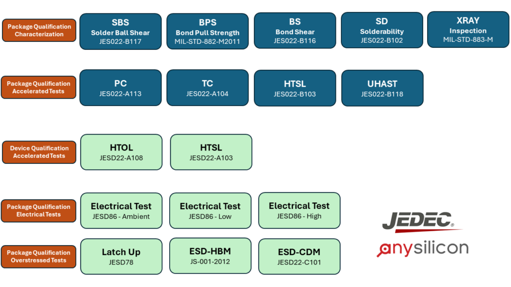
Qualification involves rigorous testing to ensure the chip meets its specifications and reliability requirements under various operating conditions. This typically includes:
Environmental Testing: Testing under extreme temperatures, humidity, and vibration.
Reliability Testing: Accelerated life testing to predict long-term reliability.
Electrostatic Discharge (ESD) Testing: Testing the chip’s resistance to ESD events.
Compliance Testing: Ensuring the chip meets relevant industry standards (e.g., automotive, medical).
Testing is crucial throughout the design and manufacturing process. Different testing methods are used at different stages:
Simulation: Verifying the design’s functionality and performance using software simulations.
Wafer Probe Testing: Testing individual dies on the wafer before packaging.
Functional Testing: Testing the packaged chips for functionality.
Reliability Testing: Testing the chips’ long-term reliability.
Packaging choice depends on factors like size, power dissipation, cost, and I/O requirements. Options include:
QFN (Quad Flat No-leads): Small, low-profile package suitable for space-constrained applications.
BGA (Ball Grid Array): High I/O count package suitable for high-performance applications.
Unit cost estimation requires detailed information from the foundry and packaging houses:
Wafer Cost: Cost per wafer divided by the number of usable dies per wafer. (use this form to receive wafer price quotes)
Packaging Cost: Cost per package. (use this form to receive IC package quotes)
Testing Cost: Cost per chip for testing. (use this form to receive IC test quotes)
Total IC unit cost = Wafer cost + Packaging cost + Testing cost
Get a fast indicative cost range, then unlock a full breakdown by email.
Semiconductor freelance and subcontractors are essential for fabless startups due to the specialized expertise and equipment required for chip manufacturing and testing. They handle:
References:

