

In this article, we delve into the intricacies of selecting the ideal semiconductor process node, providing you with valuable insights and considerations to navigate this challenging landscape. Whether you’re a seasoned professional or just starting your journey in the semiconductor industry, this guide aims to demystify the process of choosing the most suitable process node for your specific application.
In the ever-evolving world of semiconductor technology, choosing the right process node is a critical decision that can shape the success of a project. With the constant drive for smaller, faster, and more power-efficient devices, designers and engineers are faced with a myriad of options when it comes to selecting a semiconductor process node. Each process node presents its own set of advantages and challenges, making the decision-making process increasingly complex.
There are quite a few considerations that go behind deciding an appropriate semiconductor process technology node for your SoC or ASIC product. Ever wondered why did the process technology node started from 250 nm, then 180 nm, then 130 nm followed by 90 nm and so on? A little history of the semiconductor industry will help us answer that question.
In 1965, Gordon Moore, the founder of Intel, stated that every 12 months, the packing density of the integrated circuits would double. This is also referred to as Moore’s Law and it was based on an empirical observation made from the production data. Later in 1975, Moore revised the forecast of doubling the packing density every 24 months. Moore’s Law has stood the test of time and has served as a target for the semiconductor industry to pack more transistors, thereby allowing more performance to fit within the same silicon area or in other words get more performance per sq unit area. In order to keep up with Moore’s Law, foundries strived to shrink the standard cell size by shrinking the feature size of the transistors.
Looking at the process technology nodes from one generation to the next, the scaling factor has roughly been 0.7.
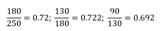
If all the feature sizes of the transistors are shrunk by a factor of 0.7, one would be able to shrink the standard cell area by roughly a factor of half.
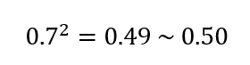
That’s the reason we typically saw the feature sizes of the transistors shrink by a factor of 0.7. Following are the factors to consider while choosing a semiconductor technology node:
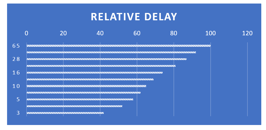
Performance of a semiconductor usually refers to the maximum frequency at which the design can operate. A higher frequency would result in higher throughput, though it may come at the cost of increased power dissipation. The scaling of the process technology node allows the feature sizes of the transistors to scale down. With shorter channel length, an electron can travel from the source to the drain in a shorter time, thereby improving (reducing) the delay of the standard cells and allowing the designs to operate at a shorter clock period. The graph below shows the relative delay with technology scaling.
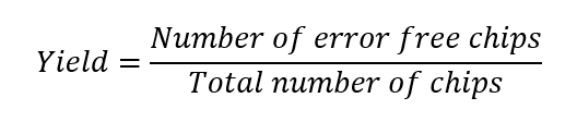
Yield of a semiconductor process is a quantitative measurement of efficiency of the semiconductor manufacturer and it is the fraction of functional and error-free chips produced divided by the maximum number of chips that could have been produced on a single wafer.
A new process node often has a low yield to begin with. Foundries strive to improve the design yield by analyzing the defects, improving the process- whether that be with respect to designing and upgrading the equipment or optimizing the use of chemicals, fine tuning the DRC decks to modify the design for better manufacturability, and having a tighter control over the environmental variables.
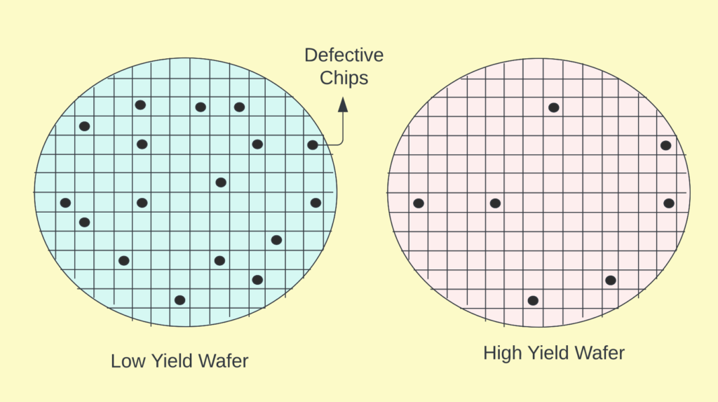
Yield is directly related to the production cost, product quality and profitability of the semiconductor industry.
Another parameter that defines the manufacturing quality of the product is defective parts per million (DPPM). It refers to the maximum number of defective parts shipped for every million parts shipped to the customer. A very low DPPM is extremely critical for semiconductors catering to aerospace, military, medical and automotive applications where a system failure can potentially have a catastrophic impact.
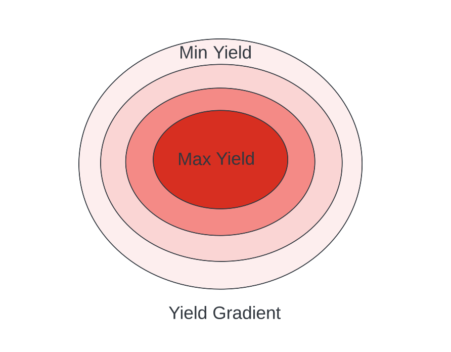
As a rule of thumb, the center of the silicon wafer usually results in a higher yield in contrast to the edge of the die because the process variations are larger along the edge.
The picture below shows the yield gradient, where the die exhibits maximum yield at the center and minimum yield along the edge. The absolute numbers evolve as the technology matures, but the trend is typically the same.
Manufacturing and design costs are functions of yield, cost of the manufacturing equipment, cost of the various chemicals used during fabrication, cost of the tester to test the fabricated design etc. This cost is high for a new technology node because it entails the need for sophisticated equipment, requires more masks to fabricate the chip and the yield may initially be low. A cost-conscious design company may need to weigh the pros and cons of moving to a newer technology while keeping the cost factor in mind. Higher packing density in a lower technology may also help offset the cost of expensive equipment.
Any design contains many different IPs like the Central Processing Units (CPUs), or Graphical Processing Units (GPUs), Power Management Units (PMUs), DSP (Digital Signal Processors), other Memory or Custom Logic and Analog Blocks. Having all the components on the same die allows tighter packing density. However, all these IPs should be available in the desired technology node or perhaps re-synthesized in the desired technology node. Availability of one or more these IPs may influence a design house’s decision while choosing a process technology node.
Get IP cores price from world class vendors.
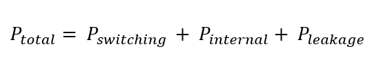
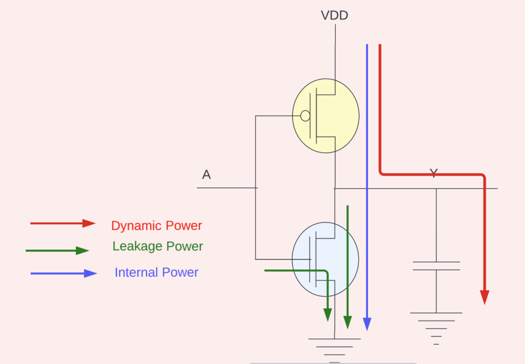
Power Dissipation has been a major concern for semiconductor design companies and customers for more than a decade now. It has 3 major components: the dynamic power, the internal power and the leakage power.
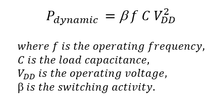
Dynamic Power refers to the power dissipated when the standard cells are switching. It is a function of the output load, operating voltage and the switching activity. Internal power is the power component dissipated when both the pull-up network (PUN) and the pull-down network (PDN) are ON for a short time. Leakage power is incurred when the standard cells are not switching and is a function of temperature, gate oxide thickness and the threshold voltage of the devices.
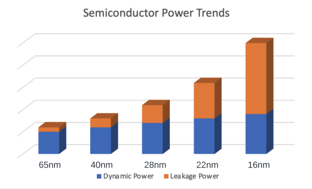
With the shrink in the technology node, the total power dissipation has been increasing. Following graph shows the dynamic and leakage power trends with scaling. While the dynamic power has increased linearly with scaling the leakage power has increased exponentially.
In order to keep the design power dissipation in check, designers have come up with innovative techniques like clock gating, power gating, dynamic voltage and frequency scaling. This adds to the design complexities and might also impact the time to market.
Design houses may choose between the three main technologies offered by the foundries after weighing their respective pros and cons:
Bulk CMOS: Bulk CMOS is the traditional technology that was easy to manufacture in high volumes. The disadvantage was the high standby power dissipation and was therefore replaced by the FINFET technology.
FINFET: FINFETs refer to fin-shaped field-effect transistor, and it offers better control over leakage by reducing the source-to-drain channel length by increasing the height of the gate above silicon substrate level. The production costs though are significantly higher than that of the bulk CMOS technology.
FDSOI: Fully depleted silicon on insulator is a planar MOS technology and therefore results in greater continuity with planar bulk as compared to the FINFET transistors which are vertical while offering the low leakage just like FINFET. Read more.
—
The mobile phones of the 21st century have more computing power than the supercomputers of the 1980s which used to take up an entire room. Scaling allows designs to pack more devices, and hence more features on the same silicon area. With the aim of making this compute power available to users whether that be to stream movies, play video games or run multi-threaded applications, higher device density would translate into smaller devices.
Some designs tend to be cell dominated like the CPUs or GPUs. While other designs tend to be routing dominated like the Crossbars. Older process nodes like 250nm had 5 layers of metal stack, while modern technology nodes like 4nm have up to 15 layers of metal stack, thereby offering more routing resources for routing the wires in the design. Though the total size of the design may be a few sq mm, the overall length of the physical routes may be several hundred kilometers for a design like a microprocessor.
A shorter time to take your design from the conceptual phase to launching a product in the market is always the goal. Any delay might result in losing the business to competitors, losing opportunities and the risk of your design not being novel. Design houses might need to weigh trade-offs while choosing a technology that is stable enough to allow them to launch their products in the market at the earliest without compromising on the yield and reliability.
In a nutshell, there are contrasting and conflicting parameters at play while choosing a process technology node. While newer technology nodes offer better performance, but it comes at the cost of increased power dissipation, perhaps lower yield but offering high packing density. Design houses need to understand these trade-offs and work with their foundry vendors and EDA partners to choose the right technology node for their products.


