


IC Insights recently released its March Update to the 2021 edition of The McClean Report. In addition to presenting its 2021 IC market forecast revisions by product type and rankings of the top 40 IDM and top 50 fabless IC suppliers in 2020, the Update contains semiconductor industry capital spending forecasts by company for 2021
Read More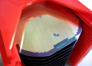
The success and proliferation of integrated circuits has largely hinged on the ability of IC manufacturers to continue offering more performance and functionality for the money. Driving down the cost of ICs (on a per-function or per-performance basis) is inescapably tied to a growing arsenal of technologies and wafer-fab manufacturing
Read More
All electronic devices we use today ranging from cell phones, TV, computers, smart speakers, have one thing in common in their manufacturing process namely Silicon Wafer.
Silicon wafers are thin slices of pure crystalized silicon. These pure forms of wafers are normally called undoped or intrinsic silicon wafer. One

IC Insights recently released its new Global Wafer Capacity 2021-2025 report that provides details, analyses, and forecasts for IC industry capacity by wafer size, process geometry, region, and product type through 2025.
Rankings of IC manufacturers by installed capacity for each of the wafer sizes are shown in Figure 1. The
IC Insights recently released its new Global Wafer Capacity 2021-2025 report that provides in-depth detail, analyses, and forecasts for IC industry capacity by wafer size, process geometry, region, and product type through 2025. Included in the report is a ranking of the 25 largest wafer capacity leaders in terms of monthly
Read More
ILPITAS, Calif., Feb. 2, 2021 /PRNewswire/ — Worldwide silicon wafer area shipments in 2020 increased while revenue remained unchanged from 2019 at $11,170 million, the SEMI Silicon Manufacturers Group (SMG) reported in its year-end analysis of the silicon wafer industry. Silicon shipments totaled 12,407 million square inches (MSI), compared to 11,810 MSI shipped in
Read More