


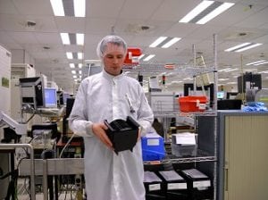
This weeks, Taiwan’s foundries and OSAT’s reported their August revenue. TSMC showing very strong year on year (YoY) growth due to it’s dominance of advanced technology for AI and smartphone applications.
TSMC Dominates with Advanced Technology
TSMC, the world’s largest contract chipmaker, reported August revenue of US$7.8 billion, a

Okmetic is currently building a fab expansion, that will more than double our Vantaa site capacity. The fab expansion will be in operation in 2025 and focus on 200 mm crystal growth as well as 200 mm SSP and DSP wafers.
Vantaa site in summer 2024
In addition
Today, GaN is set to be an indispensable technology for power and RF applications in the coming years. Established Si and SiC companies are eager to enter this emerging market, but moving from innovation to mass production raises significant challenges. Last June, Ezgi Dogmus from Yole Group, along with
Read More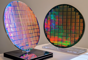
Munich, Germany and Villach, Austria – 11 September 2024 – Infineon Technologies AG (FSE: IFX / OTCQX: IFNNY) today announced that the company has succeeded in developing the world’s first 300 mm power gallium nitride (GaN) wafer technology. Infineon is the first company in the world to
Read More
September 9th 2024, SILICON VALLEY, Calif. and MALTA, N.Y., September 9, 2024 – GlobalFoundries (Nasdaq: GFS) (GF) and Silicon Catalyst, the world’s only incubator+accelerator focused exclusively on semiconductor solutions, today announced that GF has joined the incubator’s semiconductor startup ecosystem as a Strategic Partner and an In-Kind Partner (IKP). The partnership will
Read More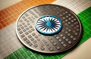
Mumbai, India September 6th 2024– The Maharashtra cabinet has approved the establishment of a semiconductor fabrication unit in Panvel, Mumbai, to be jointly developed by the Adani Group and Israel-based Tower Semiconductor. The project, which requires approval from the central government’s India Semiconductor Mission (ISM), will involve an investment of approximately
Read More