

Chiplets are a relatively recent advancement in semiconductor technology that involves breaking down a traditional monolithic integrated circuit (IC) into smaller, individual semiconductor components or “chiplets.” These chiplets can be designed and manufactured independently, and then they are integrated onto a common substrate or package to create a more complex and functional system-on-chip (SoC). The concept of chiplets has gained significant attention in the semiconductor industry due to several advantages and potentials they offer.
Looking for a chiplet try this form.
Here are some key aspects and potential benefits of chiplets as a semiconductor solution:
Modularity and Reusability: Chiplets enable modularity in semiconductor design. Instead of designing a single, monolithic chip for a specific application, chip designers can create standardized chiplets that serve various functions, such as CPUs, GPUs, memory controllers, or accelerators. These chiplets can be reused across different chip designs, reducing development time and costs.
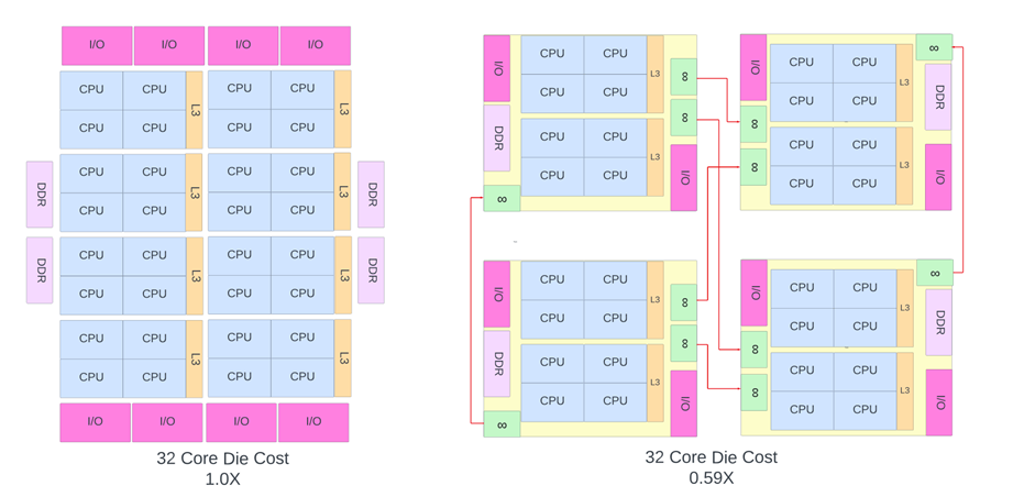
Figure 1: Monolithic Die (left) and the corresponding Chiplet Solution for a 32 Core design
Improved Manufacturing Yield: As transistors shrunk to nanoscale dimensions, manufacturing became increasingly complex and expensive. The likelihood of defects in larger monolithic chips grow, leading to lower yields. Smaller chiplets have a higher chance of being manufactured without defects, resulting in higher yields. When a single monolithic chip has defects, the entire chip becomes unusable, but with chiplets, only the defective component needs to be discarded, reducing waste and increasing overall yield.
Advanced Process Node Integration: Semiconductor manufacturing advances are costly and time-consuming. With chiplets, different components can be manufactured using the most appropriate and advanced process nodes independently. This allows for more efficient integration of cutting-edge technologies into a chip without requiring the entire chip to be manufactured using the same node. As an example, the compute chiplet that is responsible for high-performance computing tasks can be manufactured using the most advanced process node available, while the memory controller chiplet may be manufactured using a mature and a well-established process node.
Heterogeneous Integration: Chiplets facilitate the integration of different types of semiconductor technologies, including different materials and architectures, onto a single package. This enables the creation of highly specialized and optimized chips for specific tasks, such as combining CPU, GPU, and AI accelerators in a single package for improved performance in data centres or mobile devices.
Flexibility and Scalability: Chiplets offer scalability options. Manufacturers can design chips with varying numbers of chiplets, allowing them to target different markets and performance levels without starting from scratch for each product. This flexibility is particularly useful in applications like data centres and IoT devices and allows many product configurations from a single tape-out.
Reduced Time-to-Market: Moore’s Law is not only about transistor scaling but also about delivering improved performance and capabilities to consumers at a rapid pace. Since chiplets can be pre-designed and tested independently, they can significantly reduce time-to-market for new semiconductor products. This is crucial in fast-paced industries where staying ahead of the competition is essential.
Power Efficiency: By designing specialized chiplets for specific functions, power efficiency can be optimized. For example, AI accelerators can be designed to perform AI tasks with high energy efficiency, reducing power consumption in data centres and portable devices. As an example, CPU chiplet may be designed using state-of-the-art process node that excels in power efficiency while the memory controller and cache chiplet may use a process node with low leakage power.
Cost Efficiency: Chiplets are a cost optimization solution in semiconductor design, breaking down complex integrated circuits into smaller, specialized components. These modular chips can be manufactured more efficiently and economically, reducing production costs and improving yields. By mixing and matching chiplets for various functions, manufacturers can achieve greater flexibility and cost-effectiveness in designing high-performance, custom semiconductor solutions.
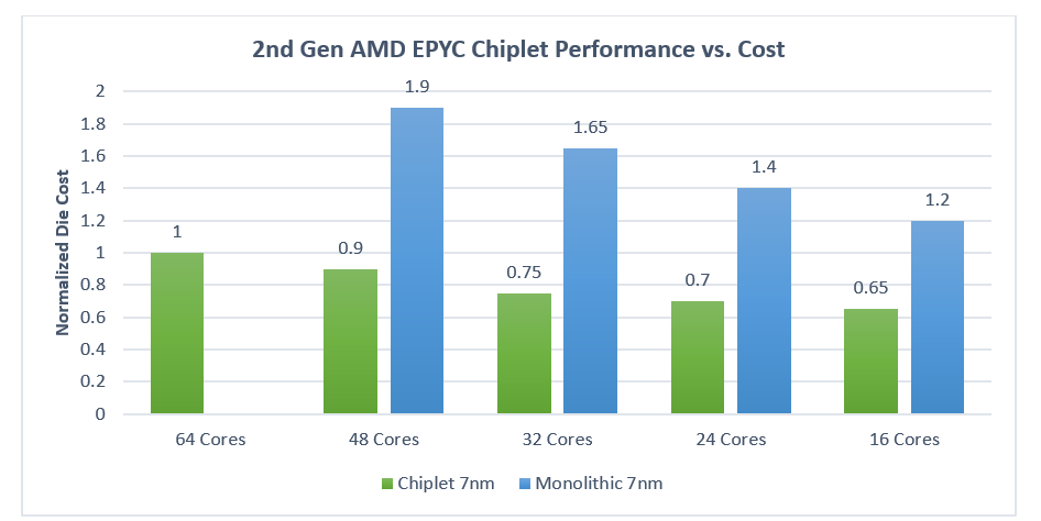
Figure 2: Cost Comparison of monolithic vs chiplet solution for 2nd GEN AMD EPYC CPU
Chiplets offer numerous advantages in semiconductor design, but they also come with their set of challenges:
Interconnect Complexity: Managing high-speed interconnects between chiplets can be complex, requiring advanced packaging technologies and careful design to ensure reliable communication.
Testing and Validation: Coordinating the testing and validation of individual chiplets, as well as the integrated system, adds complexity to the manufacturing process.
Thermal Management: Efficiently dissipating heat generated by multiple chiplets in close proximity can be challenging and may require innovative cooling solutions.
Integration Complexity: Chiplet-based designs can be more complex for designers, who must manage heterogeneous components and optimize their integration.
Despite these challenges, chiplet technology continues to evolve, with ongoing efforts to address these issues and leverage the benefits it offers in terms of modularity, performance optimization, and customization in semiconductor design.
Wafer management in chiplet-based designs is crucial for ensuring efficient production, high yield, and consistent quality. Here are three key options for managing wafers in chiplet-based semiconductor manufacturing:
Batch Processing with Advanced Packaging: In this approach, chiplets are fabricated on individual wafers using a variety of process nodes, each optimized for the specific function of the chiplet. Once the chiplets are complete, they are then combined onto a common substrate or package using advanced packaging techniques. These chiplets may come from different wafers, each with its own set of chiplets designed for specific purposes.
Multi-Wafer Fabrication with Homogeneous Integration: In this approach, multiple wafers with chiplets are processed simultaneously using a uniform process node. The chiplets may be identical or slightly customized for specific functions. After fabrication, these chiplets are integrated onto a common substrate or package. This approach is often used in cases where chiplets are similar in terms of process requirements.
Hybrid Approach with Heterogeneous Integration: This approach combines chiplets fabricated using different process nodes with those manufactured using the same process node. The chiplets on the same process node may be fabricated on a single wafer, while others from different process nodes are integrated separately. This approach offers a balance between performance optimization and manufacturing efficiency.
The choice of wafer management option depends on the specific requirements of the chiplet-based design, including performance goals, customization needs, manufacturing capabilities, and cost considerations. Each option has its advantages and considerations, and semiconductor manufacturers carefully evaluate these factors to determine the most suitable approach for their particular applications.
Integration of Chiplets
Chiplet integration involves combining multiple semiconductor chips, each serving a specific function, onto a single package or substrate. Here are some common types of substrates used for chiplet integration:
Chiplets on Organic Substrate: These are typically printed circuit boards (PCBs) made of organic materials like fiberglass-reinforced epoxy. They are cost-effective and commonly used for chiplet integration in consumer electronics.
Chiplets on Silicon Interposers: Silicon interposers are made from silicon wafers and provide a high-density platform for integrating chiplets. They offer excellent electrical performance and are used in high-performance computing applications.
Chiplets on active silicon: Interconnecting chiplets on active silicon involves designing and implementing advanced packaging and interconnect technologies, such as high-speed interposers, through silicon vias (TSVs), and microbumps. These interconnects enable efficient communication between chiplets.
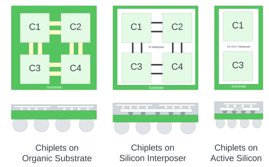
Figure 3: Chiplet Integration
Testing chiplets and testing monolithic System-on-Chip (SoCs) differ significantly due to the modular nature of chiplet-based designs. Testing chiplets presents several challenges due to their complexity:
Interconnect Testing and Validation: Ensuring the reliable communication and data transfer between chiplets is one of the most significant challenges in chiplet testing. High-speed data links and complex interconnects require thorough testing to guarantee proper functionality. Chiplets often use high-speed interfaces like SerDes (Serializer/Deserializer) or HBM (High-Bandwidth Memory), which demand advanced testing solutions to validate signal integrity, latency, and error handling. Failures in interconnect testing can lead to communication issues between chiplets, compromising the overall performance and functionality of the chiplet-based device.
Testing Across Different Process Nodes: Chiplets from various process nodes may be integrated into a single package. Testing chiplets manufactured using different process nodes adds complexity, as each node may have unique characteristics. Ensuring that chiplets with varying transistor sizes and characteristics work together seamlessly requires specialized testing methods and equipment. Inconsistent testing practices across different process nodes can result in performance disparities or compatibility issues, undermining the advantages of chiplet-based designs.
Heterogeneous Integration Testing: Heterogeneous integration, which combines chiplets with diverse functionalities and designs, introduces complexities in testing as these chiplets must work harmoniously. Ensuring that chiplets with different power envelopes, thermal characteristics, and performance requirements function together efficiently demands thorough testing. If heterogeneous integration testing is not executed meticulously, it may result in power inefficiencies, suboptimal performance, or system instability.
Addressing these challenges in chiplet testing requires advanced testing methodologies, specialized equipment, and rigorous quality control processes. Overcoming these challenges is essential to realize the full potential of chiplet-based semiconductor devices and ensure their reliability and performance.
Testing chiplets involves multiple stages, including intra-die testing, inter-die testing, and package testing. These tests ensure the individual chiplets, the communication between chiplets, and the overall packaged chiplet-based device meet quality and performance standards. Here’s an explanation of each type of testing:
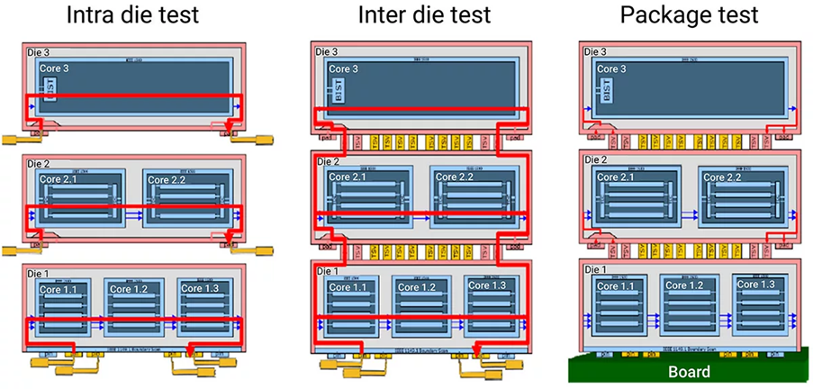
Figure 4: IEEE 1838 test access architecture for chiplet testing
Intra-Die Testing: Intra-die testing focuses on the testing of each individual chiplet before they are integrated onto a common substrate or package. This testing phase assesses the functionality, performance, and quality of each chiplet in isolation.
Inter-Die Testing: Inter-die testing focuses on the communication and interaction between chiplets when they are integrated onto a common substrate or package. It evaluates how chiplets exchange data and coordinate their functions.
Interconnect Testing: Ensures that the interconnections between chiplets function correctly and reliably.
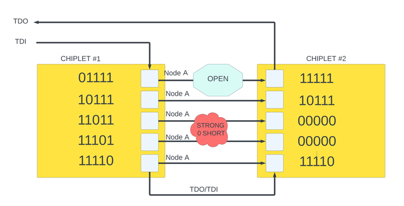
Figure 5: Chiplet Interconnect Testing using Boundary Scan
Data Transfer Testing: Evaluates the speed, accuracy, and error handling of data transfer between chiplets.
Coordinated Functionality: Verifies that chiplets work together seamlessly to perform complex tasks.
Package Testing: Package testing assesses the chiplet-based device as a whole, including all chiplets and the substrate or package that houses them. It evaluates the system’s overall functionality, performance, and quality.
Overall, these three types of testing (intra-die, inter-die, and package testing) are essential for validating the functionality, performance, and quality of chiplet-based semiconductor devices. They help identify and rectify issues at different stages of the manufacturing process, ensuring that the final product meets the desired standards and customer expectations.
The cost of chiplets in semiconductor manufacturing is influenced by several factors, including yield rates. It’s essential to compare the cost and yield of chiplets with that of large monolithic chips to understand their relative advantages and disadvantages:
Yield Impact on Cost: Chiplet production costs are significantly affected by yield rates. Lower yields result in the need to manufacture more chiplets to obtain the desired number of functional components, leading to increased costs due to the production of non-functional chiplets. Chiplet designs, with their modular nature, often lead to better yield rates compared to monolithic chips. Monolithic chips have a single integrated design, making them more susceptible to yield issues. If a defect is found in any part of the chip, the entire chip may be unusable, which can result in higher waste and production costs.
Manufacturing Complexity: Chiplets are modular and can be manufactured individually, often in smaller foundries or fabrication facilities. This modularity allows for more straightforward production processes and flexibility in selecting different manufacturing technologies for specific chiplet functions, potentially reducing costs. Monolithic chips, on the other hand, are complex and require advanced and specialized manufacturing processes, often limited to larger foundries. This complexity can result in higher manufacturing costs.
Testing and Quality Control: Chiplets, with their individual testing and compatibility checks, can have higher testing and quality control costs on a per-chip basis. However, they benefit from potentially higher overall system yield, as defective chiplets can be replaced during assembly, reducing the cost of system-level yield losses. In contrast, monolithic chips may have lower per-chip testing costs due to streamlined testing processes and economies of scale, but they are more susceptible to yield issues, which can lead to higher overall production costs if defects are detected late in the process.
In summary, chiplets offer significant potential in the semiconductor industry by providing modularity, reusability, advanced integration capabilities, and scalability. They have the potential to address many of the challenges faced by traditional monolithic chip designs, making them a promising solution for future semiconductor developments across various applications.
References:
