

A vast majority of modern digital integrated circuits are synchronous designs. They rely on storage elements called registers or flip-flops, all of which change their stored data in a lockstep manner with respect to a control signal called the clock. In many ways, the clock signal is like blood flowing through the veins of a human body while performing many critical functions. Naturally, the clock signal has a profound impact on many performance, power and area (PPA) metrics of the chip that can make the part competitive or simply dead in the water.
The clock signal needs to be routed from the source of the clock (could be the output of a Phase-Locked Loop, in context of an SoC or it could be output of a clock divider, in context of a hierarchical design) to all the sinks pins- which includes registers, latches, clock gates and macro clock pins. This is referred to as clock tree synthesis (CTS). Clock Tree Synthesis follows right after the Placement step in the physical design flow and precedes the Routing step. This post is divided into 4 sections. In the first section, we will look at various parameters that can help measure and quantify the quality of the clock tree. Next, we will introduce various clock tree architectures and talk about their trade-offs. In section III, we will discuss crosstalk noise on the clock tree network and ways to minimize the impact and the pessimism associated with noise. Finally, we conclude the post with some best known methods to achieve an optimal clock tree for your design.
Clock Tree Synthesis aims to minimize the routing resources used by the clock signal, minimize the area occupied by the clock repeaters while meeting an acceptable clock skew, a reasonable clock latency and clock transition time. Minimum Pulse Width and duty cycle requirements need to be met for all the sequential elements in the design. Lastly, the clock tree design needs to ensure that the clock power is reasonable and within the spec. We will look at all these parameters that help qualify the clock tree in detail:
Clock Latency – Clock latency refers to the arrival time of the clock signal at the sink pin with respect to the clock source. In context of a hierarchical design, the clock source may lie outside the block and the clock latency up to the port or pin on the block boundary is referred to as source latency. The clock latency from the port up to the sink pin is referred to as the network latency.
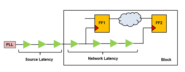
Figure 1: Source Latency vs Network Latency
Clock Skew – Clock Skew refers to the difference in the clock arrival time between two registers. It can further be sub-divided into Local Clock Skew and Global Clock Skew:
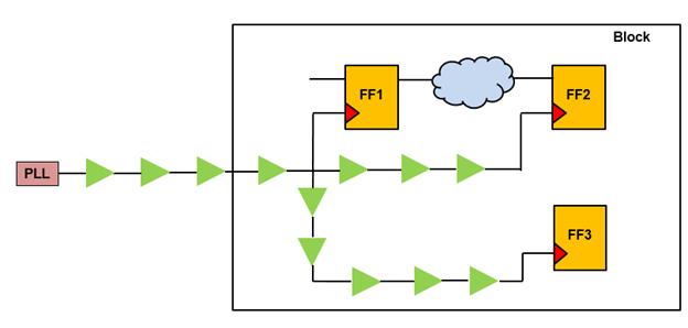
Figure 2: Local Clock Skew vs Global Clock Skew
Looking at figure 2, the difference in the clock arrival times of FF1 and FF2 is local clock skew, since these two registers have a valid timing path between them. Global clock skew would be the difference in the clock arrival times between FF1 and FF3 or FF2 and FF3, whichever greater, would be the global skew. Designers usually care about the local clock skew because it directly impacts the timing, however, global clock skew can be a useful metric to gauge the overall quality of the clock tree.
Clock Slew (or transition time): The time that a given signal takes to rise from a level of 10% of the rail voltage to the level of 90% of the rail voltage is referred to as rise slew. Similarly, the time that a given signal takes to fall from a level of 90% of the rail voltage to the level of 10% of the rail voltage is referred to as fall slew. Clock slew directly impacts the internal or the short-circuit power dissipated within the clock network, which is dissipated when current flows directly from the supply into the ground when both PUN (Pull-Up Network) and PDN (Pull-Down Network) are on. Sharper (numerically lower) slews mean PUN and PDN are simultaneously on for a shorter duration, hence lower internal power. One might argue that they can use big clock drivers to ensure sharper transitions. But this will come at the cost of area (hence leakage power) and also the switching power.
Minimum Pulse Width: All sequential elements in the design- that includes registers, latches and memories have a minimum pulse width requirement for the clock signal. The min pulse width requirement is necessary to meet to allow circuitry internal to a register, latch of an SRAM to complete their operations before being able to capture a new data or make the data available at their output pins in a reliable manner. This requirement for the pulse width may exist in the form of high pulse width and low pulse width or also in the form of minimum clock period.
As an example, for registers, the min pulse width is determined by the sum of its setup and hold time. For a positive edge triggered register, the minimum low pulse is governed by its setup time and the minimum high pulse width is governed by either its hold time or clock to output delay, whichever is higher. For SRAMs, the computation is far more complicated and it largely depends on how the memory is banked internally. But as a rule of thumb, a bigger memory usually requires a bigger min pulse width in contrast to a smaller memory because it needs more time to complete its internal operations.
Duty Cycle Check: Let’s first try to understand what causes a duty cycle of the clock signal to be distorted. Unequal rise and fall times of the clock repeaters is the primary cause of duty cycle distortion. Designers have the choice between buffers and inverters to build the clock tree. Buffers are nothing but back to back inverters, with the first inverter being small because it drives a smaller distance only to the next inverter. The second inverter is designed to be bigger because it needs to drive a long wire comprising of the RC network and/or a large fan-out. This asymmetry cause the rise and the fall edges to be skewed and depending on the number of repeater stages between the clock source and the clock sink, this difference builds up. This is the primary reasons why designers prefer to use inverters or perhaps symmetrical clock buffers to build the clock tree.
Clock Power: Clock power is typically a major component of the overall dynamic power dissipated in the design. The fact that clock signal typically has the highest frequency in the design is one reason why designers need to be mindful of the clock power. Physical design engineers have quite a few techniques at their disposal to try and reduce the overall clock power.
Clock Gating: By turning off the clock to the registers that are idle, designers can save the internal power dissipated within the registers. Clock Gating cell (also commonly referred to as integrated clock gating cell or ICG) are employed for this purpose. Clock gating can be coarse grained and fine grained. Coarse grained clock gating is usually controlled or determined at the architectural level, where one clock gate may turn off the clock to an entire module. Fine grained clock gating controls when to shut the clock to a small bunch of registers like a very small sub-module or a bus within a bigger module. And it’s also common to have intermediate levels of clock gating as well.
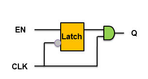
Figure 3: Clock Gating Integrated Cell
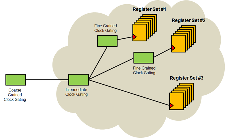
Figure 4: Coarse, Intermediate and Fine Grained Clock Gating
Use of multi-bit registers: Multi-bit registers are bigger registers with 2 or 4 or 8 registers compressed into one big standard cell. This translates into two key advantages- one being area. The area of a multi-bit register is up to 20% lower in contrast with the standalone register area, which allows designers to compress the floorplan, perhaps shorten the length of clock nets and therefore save clock power. Another key advantage comes from reduction in the clock pin cap that is exposed to the clock tree synthesis engine which directly translates into fewer clock repeaters being used and therefore saving on clock power.
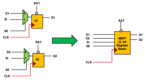
Figure 5: Using multi-bit registers imply fewer clock pins to route the clock to
Depending on the application, the clock frequency and the available resources in terms of area and routing there are three broad clock tree architectures:
Single Point Clock Tree Synthesis – This is the simplest clock tree architecture that offers lowest clock switching power but local clock skew can be fairly large. Single Point CTS is most suitable for low frequency applications, or designs with multiple clock domains. Most of the SoC applications use single point CTS. The clock divergence point begins from the clock source itself, and therefore the OCV (on-chip variation) penalty for the single point CTS is maximum of all clock tree architectures.
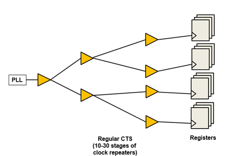
Figure 6: Single Point CTS
Clock Mesh – Clock Mesh lies at the opposite end of the spectrum that offers impeccable clock balancing, resulting in small clock skews thereby making this the choice of architecture for high-frequency GHz applications, particularly with a single clock domain. CPU and GPU applications tend to use clock mesh. The biggest disadvantage of clock mesh architecture is that depending on the density of the clock mesh, it can take up plenty of routing resources. Clock mesh cannot be gated and it tends to be highly capacitive and therefore is power hungry. The common clock path extends up to the mesh, and therefore it incurs minimum OCV penalty.
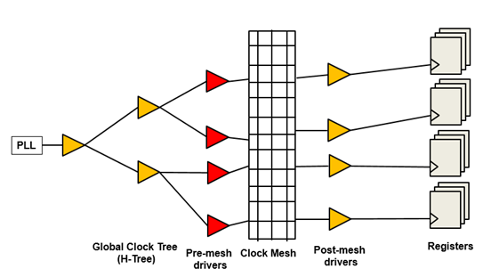
Figure 7: Clock Mesh
Multi-Source Clock Tree Synthesis (MSCTS) – MS-CTS is a hybrid approach that tends to offer better clock skews in contrast with single point CTS while at the same time doesn’t dissipate as much power as a clock mesh design. As the name suggests, it splits the design into multiple partitions, and has one clock TAP point for each partition. The clock from the clock port to these TAP points is routed with the help of an H-Tree. The multiple TAP points subsequently act as clock sources for all the sink pins within their respective partitions. The global clock tree part, as shown in Figure 5 can be a coarse mesh or an H-tree structure. The common clock path for an MS-CTS design is therefore more than that of a single point CTS, and less than that of a clock mesh.
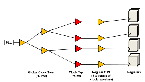
Figure 8: Multi-Source CTS
Clock signal controls and synchronizes trigger events in a synchronous design, and therefore maintaining its signal integrity is critical to meet the functional specification of your design. Crosstalk noise is the noise induced on the clock network from aggressor nets in the vicinity that may cause the clock signal to delay or make it faster or even introduce some spurious transitions called glitches.
In order to uphold the integrity of the clock network, physical designers resort to
The shielding and the NDRs do not come for free, as shielding wires add additional load cap that increases the delay on the clock tree routes while extravagant use of NDRs may cause routing congestion problems.
For multi-clock designs, it is important to understand which clocks can act as aggressors to one another. For example, one may have functional and scan clocks in the design. However, these two clocks may not co-exist- which implies that a functional clock net cannot act as a crosstalk noise aggressor for a scan clock victim net and vice-versa. By default, the analysis tools assume “infinite timing windows” for all logically asynchronous clocks and therefore that will give you pessimistic results. In addition to defining these clocks as logically asynchronous (no timing paths exist between these two clocks), one needs to define these clocks as physically exclusive (these two clocks cannot co-exist and therefore cannot can as aggressor to one another).
Another source of pessimism with respect to crosstalk noise comes from how one handles any crosstalk noise on the common clock path for setup and for hold analysis. Setup check being a next-cycle check needs to account for any crosstalk noise on the common clock path, but hold check being the same cycle check does not need to account for crosstalk noise on the common clock path.
In this section, we’ll talk about some of the best known methods to achieve the optimal clock tree.
In this post, we talked about why we need clock tree synthesis, what are the important parameters against which we measure the quality of CTS, different clock tree architectures with their respective pros and cons, discussed crosstalk noise on the clock network and ways to minimize the pessimism and finally some pitfalls or design considerations that can help designers achieve an optimal clock tree.


