

In order to cater to the computing demands for high performance computing (HPC) and artificial intelligence (AI), a need for a scalable package was felt. Chip-on-wafer-on-substrate (CoWoS) refers to the advanced packaging technology that offers the advantage of a larger package size and more I/O connections. It allows 2.5D and 3D stacking of components to enable homogenous and heterogenous integration. Previous systems faced memory limitations and contemporary data centers employ the use of high bandwidth memory (HBM) to enhance memory capacity and the bandwidth. CoWoS technology allows heterogenous integration of logic SoC and HBM on the same IC platform.
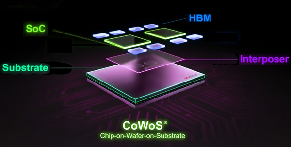
Photo inspiration: TSMC
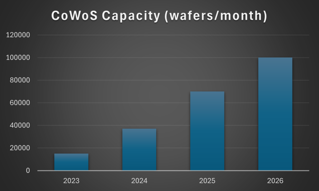
CoWoS wafer capacity is expected to grow rapidly to support the Demand for High-Performance Computing (HPC): The increasing need for advanced AI, machine learning, and data center applications requires innovative semiconductor packaging technologies like CoWoS to handle higher computational workloads.
CoWoS architecture encompasses both 2.5D horizontal stacking and 3D vertical stacking configurations, revolutionizing the traditional paradigm of chip packaging. This innovative approach allows for the stacking of various processor and memory modules layer by layer, creating chiplets that are interconnected to form a cohesive system. By leveraging through-silicon vias (TSVs) and micro-bumps, CoWoS facilitates shorter interconnect lengths, reduced power consumption, and enhanced signal integrity compared to conventional 2D packaging methodologies.
In practical terms, CoWoS technology enables the seamless integration of advanced processing units, such as GPUs and AI accelerators, with high-bandwidth memory (HBM) modules. This integration is particularly crucial for AI applications, where massive computational power and rapid data access are paramount. By colocating processing and memory elements within close proximity, CoWoS minimizes latency and maximizes throughput, thereby unlocking unprecedented performance gains for memory-intensive tasks.
CoWoS technology offers multiple advantages:
Scaling and higher levels of integration: Traditionally, scaling of transistors in accordance with Moore’s Law has helped fulfil the need for increased performance. However, this has proved to be insufficient for modern applications like high performance computing (HPC), artificial intelligence, and even graphics processing units (GPUs). CoWoS allows stacking of chips on the same substrate, therefore reducing the interconnect delays between homogenous or heterogenous logic SoCs and between the HBMs.
Enhanced thermal management: The use of silicon interposers and organic interposers have greatly enhanced the thermal management capabilities of stacked integrated circuits. This directly improves the overall system reliability, longevity while minimizing the risks of thermal throttling.
Improved Power Integrity: The use of RDLs for power/ground networks within the interposer coupled with the use of deep trenched capacitors (DTC) allow for no compromise on the power integrity for high-speed applications and memory intensive applications.
Reduction in size and cost: CoWoS technology helps mounting multiple logic SoCs and HBMs on the same interposer and substrate. This is in stark contrast to traditional packaging technologies where multiple logic SoCs used to be mounted on a printed circuit board (PCB) and make the necessary connections in the package. This resulted in bigger packages and exacerbated the material costs and manufacturing overhead. CoWoS package is overall smaller and more cost efficient.
Demand Drivers
Supply-Demand Dynamics
There are 3 class of CoWoS technologies currently in use:
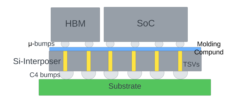
CoWoS-S: This technology uses a monolithic silicon interposer along with through silicon vias (TSVs) to facilitate direct transmission of high-speed electrical signals between the die and the substrate. The monolithic silicon interposer, however, suffers from yield issues.
Figure 1: CoWoS-S Package
CoWoS-R: This technology replaces the silicon interposer of CoWoS-S with an organic interposer. The organic interposer has fine-pitched RDL to provide a high-speed connection between the HBM and the die or even between the die and the substrate. CoWoS-R offers superior reliability and yield in contrast to CoWoS-S because the organic interposer, being inherently flexible, acts as a stress buffer and mitigates the reliability issues arising due to a mismatch between the coefficients of thermal expansion between the substrate and the interposer.
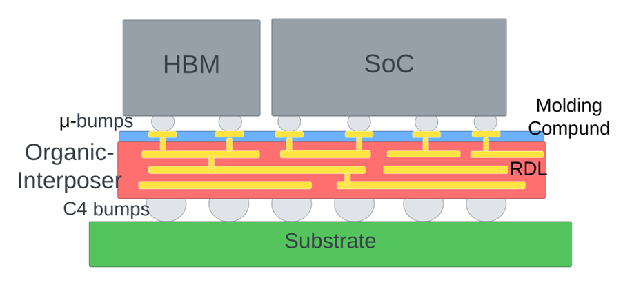
Figure 2: CoWoS-R Package
CoWoS-L: This uses local silicon interconnect (LSI) along with RDL interposer together forming a reconstituted interposer (RI). In addition to the RDL interposer, it also the preserves the attractive feature of CoWoS-S in the form of through silicon vias (TSVs). This also mitigates the yield issues arising due to the use of large silicon interposer in CoWoS-S. In some implementations, it may also use through insulator vias (TIVs) instead of TSVs to minimize the insertion loss.
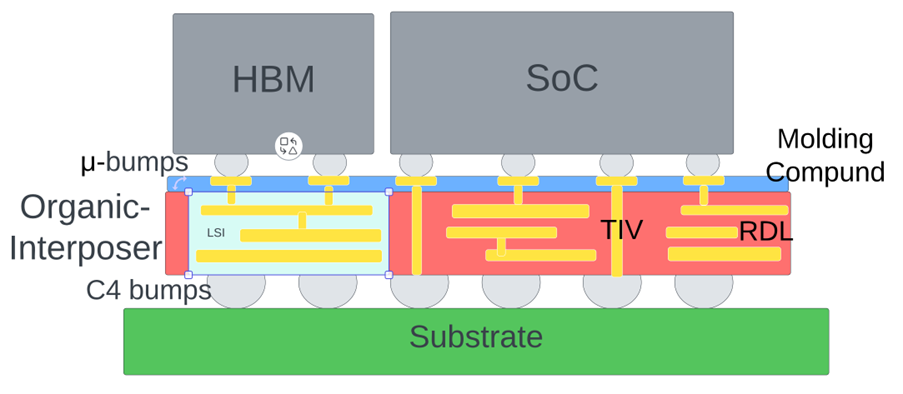
Figure 3: CoWoS-L Package
This section discusses the constituents of CoWoS-L package and the fabrication steps:
In addition to this, CoWoS-L technology also uses deep trench capacitors (DTC), which provide high capacitance density that enhances the electrical performance of the system. These capacitors act as charge reservoirs and fulfil the instantaneous current demand while running high-speed computing applications.
Manufacturing Complexity and Cost Considerations: CoWoS being a 2.5D/3D integration technique involves significant manufacturing complexity in contrast to its predecessors. The manufacturing complexity directly translates into increased cost of the chips using this package technology. This is cited to be one big reason for the increased cost of HPC and AI chips in recent times. The cost of testing a CoWoS also adds to the total cost.
Integration and Yield Challenges: 5D and 3D integrated circuits need to be tested just like any other integrated circuit to ensure that they are free of any manufacturing defects. Testing a 2.5D or a 3D integrated circuit is however far more challenging because each wafer die needs to be tested individually before mounting them on the interposer, and subsequently need to be tested again after mounting. In addition to this, the through silicon vias (TSVs) also need to be tested. Lastly, the large silicon interposers are particularly susceptible to manufacturing defects and may lead to yield loss.
Thermal Challenges: CoWoS packages suffer from thermal issues due to a difference in the coefficient of thermal expansion (CTE) between the interposer and the substrate. Using organic interposers do limit the thermal issues to some extent. The life of a solder joint can be greatly enhanced by using an underfill material which buffers the thermal mismatch between the silicon die and the substrate.
Similarly, on the front-side, the integrity of the redistribution layer (RDL) particularly underneath the two silicon dies is vulnerable to stress. The use of μ-bump underfill again acts as a stress buffer between the silicon dies and the RDL.
Electrical Challenges: CoWoS packages suffer from electrical challenges in the form of signal and power integrity issues.
(1) Signal Integrity:
(2) Power Integrity: CoWoS packages are typically used for high performance applications that have higher data toggle rates and low operating voltages. This makes these packages susceptible to power integrity challenges.
CoWoS technology can support much higher number of transistors in a package in contrast to older packaging technologies like System-in-Chip (SiP). All applications that require significant amount of parallel computing, processing large vectors of data and ones that need high memory bandwidth are most suitable to use this technology.
![]()
Figure 4: Increase in transistor count with CoWoS Development
Some of CoWos applications are:
Many companies have thrived on the success of CoWoS packages. A few examples are:
Answer a few questions and get a recommended CoWoS family (e.g., CoWoS-S/R/L).
Recommended package family: —
—
CoWoS technology offers higher levels of integration allowing for integrated circuits to scale to meet the demands of growing compute capacity. The technology is consistently evolving to ensure better yields, robust power and thermal integrity and increasing the interposer area further to allow more wafers to share the same substrate. CoWoS will continue to fuel the growth of semiconductor industry over the next few years.
