

A die per wafer calculator is a tool used by chip designers and fabs to estimate how many individual dies (aka chips) can be cut from a single semiconductor wafer.
It’s like trying to fit as many square stickers as possible on a round sheet—sounds simple, but in the chip world, it’s a game of millimeters that affects cost, yield, and scalability.
If you’re building a custom ASIC or evaluating the economics of a silicon run, calculating the number of dies per wafer accurately is a must.
Calculating the number of Dies Per Wafer (DPW) is a very simple and straight forward task. It’s actually based on basic high school mathematics which are related to circle area formula, remember Pi?
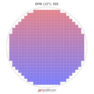
Silicon dies which are placed on a wafer can also be described as many squares placed inside a circle — thus the calculation is about first finding the overall circle area using both the mathematical number Pi (approximately equal to 3.14159) and the wafer size.
The wafer size and the die size are known in advance, however, as our “squares” have spaces between them (e.g. scribe lines) and the area located at the edge of the wafer cannot be used, the calculation is a bit tricky, therefore, some recommend using the Die Per Wafer tools results as an estimation rather than a calculation.
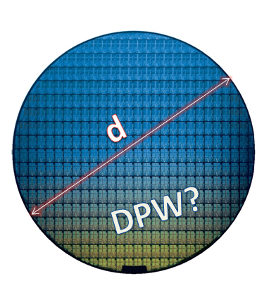
Visual representation of a silicon wafer highlighting the wafer diameter (d) used to calculate dies per wafer (DPW).
In addition to the above unused area, the foundry will use additional area for testing purposes (PCM structures) that will eat up relatively small size of the wafer. Sawing lanes, wafer margin and test structures size vary from process node to process node and from foundry to foundry. Therefore, is it highly recommended to have the final DPW figure directly from the foundry because they have all the knowledge and information required to provide the actual figure.
Every square millimeter of wafer area counts. Here’s why:
Big players like GlobalFoundries (GF) and Amkor rely on precise estimations using these calculators to plan production efficiently. So do smaller ASIC design companies and service providers.
Manual calculation vs using a calculator
Our free Die Per Wafer calculator is very simple and based on the following equation:
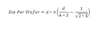
Refined die per wafer formula accounting for wafer diameter (d), die size (S), and edge losses—commonly used for more accurate DPW estimation in semiconductor manufacturing.
d – wafer diameter [mm] (click her for wafer size information)
S – die size [square mm]
For your convenient, we have placed the Die Per Wafer calculator as an online Excel sheet so you can use it online or download it into your ASIC price calculator.
Many engineers search for a die per wafer calculator Excel template. And while you can build one using basic geometry, it takes effort to include corrections for edge losses.
Instead, you can:
Some fabs also offer proprietary Excel tools, but these are often closed-source.
Think of gross die as all the chips that could fit, while net die is the realistic number after subtracting edge loss and defects.
Calculators help estimate both, but you’ll still need a die yield calculator to account for defect density and test failures.
Here’s how a standard tool like the one on AnySilicon works:
It’s fast, browser-based, and doesn’t require downloads.
Imagine placing tiny square tiles (dies) on a big round dinner plate (wafer).
That’s basically what fabs deal with—trying to pack as many functional dies as possible onto every wafer to maximize return.
Scribe lines are the tiny spaces between dies that allow for cutting. Ignoring them in your calculation can overestimate your die count by 5–10%.
Look for a die per wafer with scribe line calculator if your application needs that level of accuracy.
Whether you’re doing early-stage feasibility or planning your first tapeout, die estimation is a critical input.
Let’s unpack the math just a bit more. You already saw the basic formula:
But to get a more realistic estimate, especially near the wafer edges, we use an improved version:
This formula subtracts unusable dies near the edge (since you can’t cut perfect squares from a round edge without loss). Some calculators also add scribe line spacing into the equation.
Once you know your gross die count, you still need to consider die yield. Even if you could fit 700 dies on a wafer, not all of them will work due to:
This is where a die yield calculator comes in. The most common yield model is Murphy’s yield model:
Where:
So yeah, even a perfect calculator can’t predict the net usable dies without knowing your process conditions.
Top foundries like TSMC and GlobalFoundries don’t just estimate—they simulate. Still, they start with basic die-per-wafer math before moving to process-specific adjustments.
For example:
Even in high-volume production, this calculation remains a key cost driver.
Here’s a quick breakdown:
| Tool Type | Pros | Cons |
|---|---|---|
| Online calculator (like ours) | Fast, no setup, updated formulas | Needs internet |
| Excel sheet (like ours) |
Portable, customizable | May lack accuracy without edge corrections |
| Mobile app | Great for quick checks | Often limited in flexibility or precision |
If you’re presenting to a team or client, go with Excel or a web calculator you can show live.
If you’re in the fab or lab, having a calculator app on your phone can be handy for a rough estimate.
Let’s run through a real-world example.
Step 1:
Wafer area = π × (150)² = ~70,685 mm²
Step 2:
Gross dies = 70,685 / 100 = ~706
Step 3 (adjusted):
Subtract edge loss (~5–10%)
Adjusted dies ≈ 706 – (5% of 706) ≈ 670
So, you’ll get roughly 670 gross dies per 300mm wafer in this case.
Now plug the same values into our online calculator to confirm!
Many engineers stop at the gross die count. But remember:
Always combine the calculator with realistic yield expectations—especially during NPI (New Product Introduction).
You should be using the die per wafer calculator during:
It’s not just a math tool—it’s a strategic planning weapon.
Want to DIY an Excel calculator? Use this formula:
For better results, subtract about 10% to account for edge loss and partial dies. Or, download templates from fab-specific forums (some even share ones for die per wafer calculator 1.00 versions—ideal for older toolsets).
Yes, and it’s still useful. Many analog or MEMS designers still use 2-inch wafers. Use the same process:
Small wafers = small volume = high per-unit cost. But in some cases, that’s fine.
The die per wafer calculator is more than just a number cruncher.
It helps:
Whether you’re working with TSMC, Amkor, or a smaller ASIC design company, this tool keeps your numbers honest.
Want to skip the formulas and math?
Head over to the free die per wafer calculator and get started.
Just enter:
…and the tool does the rest.