The ams OSRAM 2026 MPW (Multi-Project Wafer) program expands its technology offering with new 180nm options, including the C18 CMOS specialty platform further enriching the MPW portfolio. For mixed-signal designs in mature nodes, this extension delivers strong analog, high-voltage and BCD capabilities tailored to customer needs.
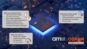
The MPW program provides design engineers with a low-entry-barrier, cost-efficient way to accelerate integrate-circuit development through fast and affordable prototyping in a high-volume, automotive-grade European full-service foundry. It supports established companies, design houses, startups, and research institutions in prototyping and validating ICs without the cost of full wafer runs, while maintaining a seamless path to high-volume production.
The MPW program is also ideal for companies looking to test designs and reduce supply-chain risks by exploring ‘local for local’ manufacturing solutions.
What is new in 2026?
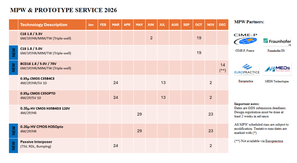
The 2026 MPW program introduces new 180nm mixed-signal CMOS and 180nm BCD (Bipolar-CMOS‑DMOS) technology platforms. These versatile 180nm technology platforms support 1.8 V/3.3 V, 1.8 V/5 V, and 1.8 V/5 V/70 V (BCD) power-supply domains. This expansion is central to ams OSRAM’s drive to be a European foundry of choice by offering reliable supply, cycle time, and trusted long-term partnerships with consistent quality and transparency.
These 180nm platforms enable a wide range of designs such as power-management ICs, motor management ICs, motor‑driver ICs, LED/laser driver ICs, actuator driver and control ICs, sensor interfaces, mixed-signal circuits, and high-voltage devices. Engineered for high reliability and performance, the 180nm platforms meet the demanding requirements of automotive and other high-performance analog applications, and are suitable for industrial, medical, consumer, security, defense and space applications.
The MPW program also continues to offer proven technologies such as 350nm CMOS, CMOS high-voltage and embedded‑flash options, giving designers flexibility across many application areas.

Global access made easy
Participation in the MPW program is made seamless and locally supported through collaboration with leading organizations and strategic partners worldwide.
These long‑standing partnerships give universities, research institutes, startups, design houses, and established companies worldwide easy access to our trusted foundry services.
Customers benefit from a one-stop‑shop that covers wafer fabrication, optional analog IP, memory generation, and delivery of diced wafers or packaged parts in ceramic or plastic packages. This integrated approach simplifies development and reduces coordination effort for engineering teams.
Automotive-grade processes trusted by major manufacturers
As a European-based foundry, ams OSRAM places quality and reliability at the core of everything we do. Our processes meet stringent automotive and industrial standards, and we provide comprehensive design support through a Cadence based Process Design Kit (PDK) that includes all essential libraries, IO cells, and analog blocks.
How to join a 2026 MPW run
Participation in an MPW run is based on a completed GDSII database submitted in line with the published tape out dates. After successful data checks and mask preparation, customers typically receive untested samples (dice and/or packaged parts) within about ten to twelve weeks, depending on the chosen process.
To join an MPW run, prospective customers follow three steps:
Next steps
The 2026 MPW calendar including process options and practical details on tape-out and deliverables, is now available on the ams OSRAM Full-Service Foundry pages. Design teams that plan early can secure a preferred shuttle slot and move faster from concept to qualified silicon.
Take this opportunity to bring your ideas to life.
Contact our MPW team: foundry@ams-osram.com
Author: Joni Jukka Krister Mellin
Biography: Principal Product Marketing Manager, Full-Service Foundry at ams OSRAM, has over two decades of experience in semiconductor and photonics technologies. His career spans engineering, business leadership, and foundry operations across ams OSRAM, X‑FAB, Nokia, Microsoft and Micro Analog Systems, backed by technical degrees from Aalto University and a dual global executive MBA.