

Today is the era of cutting-edge modern technologies. Things are becoming more advanced, smarter, and more compact continuously due to technical advancements. From smart LEDs to smart phones computer systems to electronic appliances, everything is continuously evolving because of Integrated Circuits (ICs). So, the question raised when we hear the word “IC” what is it? And how it becomes the fundamental part of every digital electronic system? Can we live without it?
An Integrated Circuit (IC) is a miniature circuit where elements like transistors, resistors, and capacitors are combined on a small semiconductor substrate, typically silicon. Transistors are the most fundamental building blocks of ICs.
Integrated Circuit or commonly known as “IC” is a type of circuit in which elements are interconnected and associated so that they cannot be separated in very small space. It means that IC itself is a large circuit which can contains several different smaller circuits. Circuit elements includes resistors, transistors, capacitors etc. The most fundamental element is transistor.
![]()
Figure 1-Commonly available Transistor
IC design is one of the most advanced and one of the most complex engineering tasks in modern world. The goal of IC design is to create a circuit which have a desired functionality. For example, an IC which can decode the incoming weather messages and notify the users.
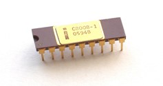
Figure 2-Intel 8008 microprocessor, arguable the first “true” microprocessor
The fundamental blocks of integrated circuit design are transistors, resistors, capacitors, and wires. These elements are interconnected to form building blocks such as logic gates, or amplifiers. Those building blocks are interconnected to form more complex designs to achieve more advanced functionality such as buffers, multipliers, flip flops etc. This process continues to develop, which results in formation of some of the most complex circuits such as microprocessors etc. The circuit elements in IC design are made from miniaturized components that are created on any semiconductor substrate (such as Silicon, Germanium) using a complex process called photolithography. This process involves creation of various geometric shapes on the substrate where the electrical properties of the region defined by the shape. These circuit elements are created when combined those geometrically shaped regions.
The IC design contains two distinct processes:
Logic Design which includes the combination of circuit elements to implement desired functionality using Computer Aided Design (CAD) or Electronic Design Automation (EDA) tools.
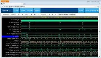
Figure 3-Waveform showing the behavior of design on EDA tools
Physical design which includes creation of those circuit elements on semiconductor substrate using the geometrically distinguished regions and their interconnection.
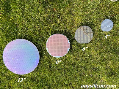
Figure 4-A Silicon wafers/substrates
There are various steps involved in an IC Design. These steps can be increased or decreased based on the functionality and complexity of the IC. But the most commonly used steps are as follow.
Architecture: This is the most fundamental and important part of the IC Design flow. Here the requirements and specifications for the design are gathered and discussed. Specs may include required speed, power consumption, targeted cost, time-to-market, required blocks, timing constraints. Here the complex design is created in form of a block diagram where the whole design is divided into multiple sub blocks. Each block represents a specific module which are interconnected. The whole functionality is divided into sub-functionalities, “which” module to achieve “what”. For example, in a microprocessor design, the design can be divided into multiple sub-modules, such as register file, ALU, control unit, address decoder, adder, multiplexers, different sort of staged pipelines, buffers and some clocking modules. Now in this phase, the functionality of each module is specified, let us say control unit is responsible for sending resets or control signal for each module, ALU is responsible for arithmetic operations, register file is responsible for holding registers and their addresses etc. In this phase, “what” is emphasized the most, not “how”. Implementation of the design is usually not the part of Architectural design phase, but it can be discussed.
Logic Design: In this phase, “how” is emphasized and well defined. Here sub modules are designed using human-understandable programming languages and interconnected to implement the desired functionality of the IC. Usually, pre-existed modules are used such as memories, storage, processing units, sensors to save time and design only the specific module which needs to be replicate the true functionality of the IC. It includes coding of RTL design in Hardware Description Languages (HDL) such as VHDL or Verilog. EDA tools such as compilers and simulators for RTL design are used to check and verify the correct functionality. Design and Verification of IC runs parallel, both includes the coding mechanism on HDLs. Design engineers are responsible for understanding the architecture and specifications whereas Verification engineers are responsible for verifying the designed RTL, to cover maximum possible corner cases.
Logic Synthesis: In this phase, RTL design is converted into netlist. Netlist is a stream of binary codes which can be load into a programmable hardware to prototype the functionality of IC on it, such as FPGA. Then the design functionality is verified here. After this, design is divided into physical blocks, means now the logic is now started to be implemented on physical layer and components, such as gate level. In parallel, timing margin and timing constraints which are decided in architectural designs are also checked and verified. RTL and gate level netlists are being verified properly. Static timing analysis is also done in this phase.
Floor planning: This phase includes the schematic representation of major functional blocks and their placement on the layout. It introduces some sort of geometrical design constraints in the IC.
Usually, power consumption is planned during the floor planning, due to the geometrical design constraints, which helps to calculate the approximate power consumption for the whole chip, as well clocking domain design for all the modules.
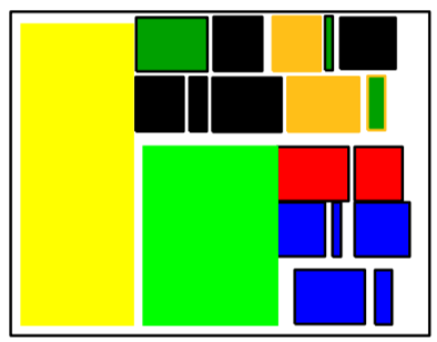
Figure 5-Floor Planning of 3D IC Design
Placement and Routing: In this phase, all the modules are interconnected, and a block level physical layout is created for placement and routing between the interconnects of modules. Here actual physical layout is not created.
Layout: This is the final phase of IC design flow. Here the actual physical layout is created by placing millions and billions of transistors together to create all sub-modules and their interconnects. GDSII file creation also occurs here which then send to the fabrication foundry from where the chip will be produced on silicon substrate using photolithography.
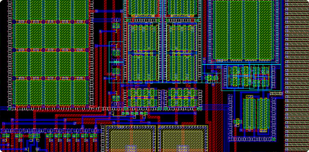
Figure 6-Layout view of a simple IC design
Fabrication: Here comes the most difficult part of IC design. The fabrication of the chip using billions of small transistors on the silicon substrate using photolithography in an Extreme Ultra-Violet (EUV) machine which is considered as on of the more innovative technical of our time. This machine together with raw silicon is the key to producing silicon wafers. Wafers consist of many millions or billions or trillions of transistors is eventually made into computer chips.
Silicon wafers are thin slices of pure crystalized silicon. These pure forms of wafers are normally called undoped or intrinsic silicon wafer. One of the reasons for using Silicon wafer in semiconductor industry is the natural abundance of Silicon. It is one of the most abundant material found on earth usually found in the form of SiO2. Another reason of using silicon is that electrical characteristics of the silicon can be precisely controlled by addition of dopants. Silicon wafers that are doped with impurities such as Boron create P- type wafers and wafers that are doped with Arsenic or Phosphorous create N-type wafers. The P type wafers have several positive charged holes whereas N type wafers have several negative charged electrons in it. The process of wafer production is described on this page.
Packaging: IC packaging is the second last stage in the IC design flow. During this stage, the IC device gets packaged to protect the IC from potentially damaging elements. In todays market, there are several types of IC packaging offering such as QFN, BGA or bumping, that would fit any type of IC design performance and cost targets.
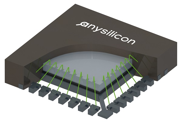
Figure 7- QFN Package
Post Silicon Validation: This is the last step of IC design flow. In this stage, IC is taped out from the foundry and its post silicon validation starts, which includes the verification of timing constraints, interfaces verification, power consumption etc. After which the chip is available in the market.
The process of designing an IC takes all these complicated steps from imagination to realization. During all the stages of IC manufacturing, there are several verification milestones to make sure that design is working as intended. If design targets and specs are violated, the manufacturing process can correct it until the chip is fabricated. The cost of correcting these issues before fabrication is directly dependent on how close we are to the fabrication step. The close the process is fabrication, the higher the price to fix the issue. Once the chip is fabricated and bug went under the radar during all verification steps, there is no simple solution to fix it, unless there are certain SW work arounds.
These are the general and commonly followed IC design flow. Several steps can be skipped or added depending upon the requirement of the chip architecture. No wonder IC design is sometimes referred as one of the “most complex engineering task mankind has ever achieved” because it seems impossible to generate and interconnect billions and trillions on transistor into something which is smaller in size than a human nail to achieve complex and desired functionality.
Interested in more information regarding IC design flow? Clock here.
