

When we say semiconductors, what is the first thing that comes to mind? Most of the time we think about computer chips and transistors, but it’s not as simple as it seems. For us to be able to get a basic understanding of the process of manufacturing semiconductors, we need to understand what a semiconductor is and what its role is in all the technology that surrounds us every day.
As defined in the Oxford English Dictionary, “a semiconductor is a solid substance that has a conductivity between that of an insulator and that of most metals, either due to addition of an impurity or because of temperature effects. Devices made of semiconductors, notably silicon, are essential components of most electronics circuits”. Here is an example to help us get a better understanding of what a semiconductor is.
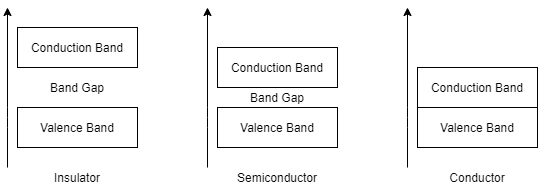
Figure 1 – Conductor/Semiconductor/Insulator sketch
Think of a piece of copper wire. That is a solid that conducts electricity, which means it allows for the easy passage of electrons through its material. On the opposite end of the spectrum, think of a rubber band. The rubber is against the passage of electrons, which means it is an insulator. Now, if you get a piece of silicon and mix in certain metals with it, you get a semiconductor, a material that is between an insulator and a conductor.
But why do we need semiconductors in the first place? Well, semiconductors are the foundation of all electronics, from the ones that you find in your phone, to the ones that you have in a microwave oven, car and even blender.
As such, they are extremely important in the existence of our society, being the building block of all the technology that surrounds us.
Before getting into the manufacturing process of such semiconductor devices, let’s have a look at the history of semiconductors, to help us better understand what a semiconductor is made of and what implications it has.
Semiconductor History
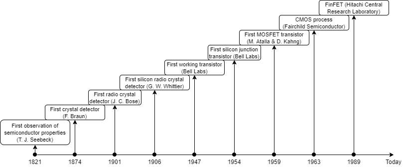
Figure 2 – Semiconductor Historic Timeline
Materials that have semiconductor properties have been observed and studied as far back as the early 19th century, with the first observer being the German physicist Thomas Johann Seebeck in 1821.
As for the first useful technologies that resemble anything we use and make today are the silicon radio crystal detector, developed in 1906 by American engineer Greenleaf Whittier Pickard, and the point-contact transistor, invented at Bell Labs in 1947 by John Bardeen, Walter Houser Brattain and William Shockley.
An important mention is that all the early semiconductor devices were quite large and bulky, very different from the tiny, close to nanoscale devices that power our lives today. Due to these disadvantages, the first semiconductor devices were used only for highly specialized and expensive equipment, as it will take a few decades for this technology to mature and become scalable and mass-produced. Only after these two conditions were met did we see the massive adoption and inclusion of semiconductors in all the fields and domains that seem obvious and natural to us today.
Semiconductor Component Elements
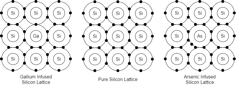
Figure 3 – Semiconductor component elements
To make a semiconductor, we need a base material, one that is stable from the electron point of view. This means it has to be from the tetravalent (meaning to have four electrons available for sharing in a covalent bond) group of elements of the periodic table. The most well-known and used element is silicon, which is very abundant and easy to work with. It is present in all types of sand, but there are certain types of sand which have an extremely high concentration of silicon.
A crystalline lattice made of silicon is very stable, but is not very conductive. That is why we need to enrich it with either trivalent (boron, gallium, indium) or pentavalent (antimony, phosphorus, arsenic) elements. Trivalent elements are called acceptor impurities and pentavalent elements are called donor impurities because of the change they cause in the crystalline lattice.
Acceptors create holes (these are just places where an electron is missing from, they are not actual particles), which then make the semiconductor become of type p (because it has more Positive charges than negative ones). Donors add electrons to the crystal lattice, which makes the semiconductor become of type n (because it has more electrons, which means more Negative charges than positive ones).
The process that combines these elements together into the actual semiconductor, it is called doping, and it is a very expensive and complex process, as the materials that enter the process need to be very pure, because even tiny atom-sized imperfections in the lattice can lead to malfunctioning electronics later on the assembly line.
Semiconductor Manufacturing Process Steps
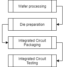
Figure 4 – Semiconductor Manufacturing Process Steps
We can split the semiconductor manufacturing process in four main steps: wafer processing, die preparation, IC packaging and IC testing. Only the first process concerns us here, as the other three steps change depending on the circuits that are being made later on.
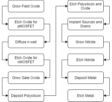
Figure 5 – Wafer processing steps example for CMOS
Wafer processing is a delicate and complex process, which has multiple steps in its own right. Wafer fabrication is used to build components with the necessary electrical structures for the end-result product (usually an integrated circuit, IC for short).
Read here about Silicon Wafer.
The main process begins with a team of engineers designing the circuit and defining its functions, all the while specifying the inputs, outputs, and voltages needed for the correct operation of the circuit. These specifications are entered into a variant of electrical circuit design software, and then imported into circuit layout applications, which, similarly to computer assisted graphics, help us get the design out into the real world.
The resolution of the circuit increases with each step in the wafer manufacturing process, as the scale at the start of the design process is already being measured in fractions of micrometers and by then end of the whole process we get to several nanometers, which is a couple of orders of magnitude smaller that at the first step.
The silicon wafers start out blank and pure. The circuits are built in layers in clean rooms (any imperfection ruins an area that houses tens of millions, if not billions of transistors, so any mistake is very expensive). Then, via the process of repeated printing, etching and metal deposition, we end up with a crude wafer, which then needs to be send to a testing area, to make sure the design has been created according to the specifications and that the purity of the wafer is within the margins of error.
The actual processes that go into wafer manufacturing are extremely complex and technical, but the key takeaway is that you start with a thin wafer of silicon, in which you “draw” your circuit at the scale of a few nanometers, then print, etch and treat the wafer. Also, the manufacturing process changes frequently, because each year new techniques and equipment is created, which shrinks the scale even more.
All these new technologies have been working to get the semiconductor devices down from a few micrometers in size (10 micrometers in 1971), all the way down to only a few nanometers in size (5 nanometers as of the end of 2020). Research is still being done in this direction, as the physical limits of semiconductors still allow us, theoretically, to go down to only a couple of nanometers.
Read more about wafer size history.
Semiconductor Manufacturing & Moore’s Law

Figure 6 – Moore’s Law
The trend has first been described by Gordon Moore, who is a co-founder of Fairchild Semiconductor and Intel. The law now known as Moore’s law started only as a prediction made in 1965, made as a contribution for the Electronics magazine’s thirty-fifth anniversary issue. Initially, it states that the number of components per integrated circuit will double every year. A revision was made in 1975 by the author, looking to the previous ten years and forecasting a doubling every two years.
Why is this important? Well, manufacturers have to keep Moore’s law in mind when they adjust their budgets for production, research and development; future predictions are very important and necessary, as the process of manufacturing semiconductors is a lengthy, intricate and expensive one.
As of 2013, the estimated cost of a building in which all these processes takes place is around $10 billion and they take between 2 to 3 years to build and ramp production. These buildings are referred to as fabs or foundries and they are extremely expensive and complicated, which is why the companies that make semiconductors need to keep a healthy prediction of the future demand in mind all the time.
We can see the implications of such a peak in demand right now. Due to a multitude of factors, semiconductor manufacturing has become a bottleneck over the course of 2020 and 2021, with estimates of getting supply back up in around 2022 at best. This silicon shortage has been caused by a couple of events, but the key elements, in regards to our own discussion here, are the faulty predictions that manufacturers made in 2019, leading up to the start of the pandemic. This, in turn, caused a back-up at the graphic card level, then it went further and further down the manufacturing stack, impacting all technology manufacturers, resulting in the current pickle of a situation.
Semiconductors Future
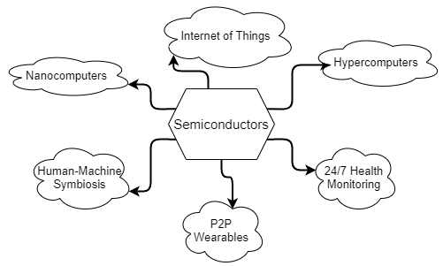
Figure 7 – Future of semiconductors
The process of manufacturing semiconductors is not something that can be easily understood and/or performed, but it is extremely important to all of us, like it or not. Semiconductors are all around us, they make up the circuits that allow us to travel vast distances, to calculate the positions of stars and galaxies, to order a pineapple pizza and to watch a movie on Netflix.
As for the future of semiconductor manufacturing, it seems rather bright. There is a lot of work and effort being put into the development of better, faster, cheaper technologies to make smaller and smaller semiconductor devices, such as transistors and MEMS (micro-electro-mechanical systems).
For the time being, we can say that Moore’s law still holds, but not in the traditional sense. The number of components is no longer doubling every two years, but the process has so many different sub-processes underlying it, and that means there are a lot of possible improvements, disruptive technologies that are being worked on now or that are not even conceived of yet.
The future of semiconductors seems promising and there sure is a long way to go before this technology reaches its physical limits. The continuous developments made in the area of semiconductor manufacturing will lead to new discoveries and uses in IoT, 24/7 Health monitoring, Hyper- and Nanocomputers (larger dies with multiple quadrillions of transistors and microscopic size dies with millions of transistors), Implantable Augments and Intelligent Wearables with Peer-to-Peer communication to name just a few.
These improvements, and all the others that we cannot even imagine, will have a tremendous impact on society and human beings. It is impossible to predict where they will take us, but we can still hope for the best! A semiconductor revolution is coming, sooner rather than later, it seems.


