18601 Views

Introduction to ASIC Design Flow

Today, ASIC design flow is a mature process with many individual steps. ASIC design flow process is the backbone of every ASIC design project. To ensure design success, one must have: a silicon-proven ASIC design flow, a good understanding of the ASIC specifications and requirements, and an absolute domination over the required EDA tools (and their inputs and outputs).


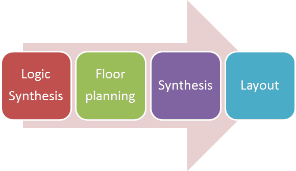
A simplified version of an ASIC design flow is described in the following diagram. Although analog ASIC design and digital ASIC design have some differences, they still share a common structured backbone.


ASIC Design Flow Step 1: Logic Synthesis


  • RTL conversion into netlist
  • Design partitioning into physical blocks
  • Timing margin and timing constrains
  • RTL and gate level netlist verification
  • Static timing analysis

ASIC Design Flow Step 2: Floorplanning


  • Hierarchical ASIC blocks placement
  • Power and clock planning

ASIC Design Flow Step 3: Synthesis


  • Timing constrains and optimization
  • Static timing analysis
  • Update placement
  • Update power and clock planning


ASIC Design Flow Step 4: Block Level Layout


  • Complete placement and routing of blocks


ASIC Design Flow Step 5: ASIC Level Layout


  • ASIC integration of all blocks
  • Place and route
  • GDSII creation


See here our previous articles that covers ASIC design flow.

Get 3 quotes from ASIC design companies for your ASIC project.

Recent Stories


Logo Image
Privacy Overview

This website uses cookies so that we can provide you with the best user experience possible. Cookie information is stored in your browser and performs functions such as recognising you when you return to our website and helping our team to understand which sections of the website you find most interesting and useful.