A Process Design Kit simplifies the complexities of chip design by providing essential resources for IC engineers, including design rules, models, and documentation. This toolkit not only streamlines the development process but also ensures that designs can be manufactured successfully with high yield rates. The semiconductor industry relies heavily on PDKs to bridge the gap between design and manufacturing, making them a crucial component of modern technology.
This comprehensive guide delves into the definition and importance of PDKs, their benefits for design engineers, and answers common questions surrounding their use. Join us as we explore the future of Process Design Kits and their pivotal role in shaping the semiconductor landscape.
Definition of a Process Design Kit (PDK)
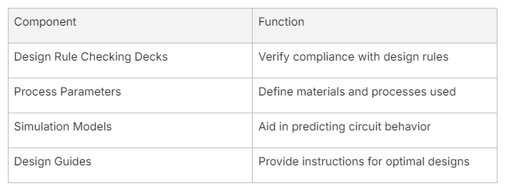
A Process Design Kit (PDK) is a crucial tool in the semiconductor industry. It serves as a bridge between the design process and manufacturing. The PDK includes design rules, design guides, and design rule checking decks. These ensure that designs comply with manufacturing capabilities.
Design flows rely on the PDK to create integrated circuits. It provides the design tools necessary for the semiconductor design process. This helps engineers optimize and verify their designs before production.
Here are key components of a PDK:
- Design Rules: Guidelines that ensure the designed circuits are manufacturable.
- Design Guides: Step-by-step instructions to aid designers in the process.
- Checking Decks: Tools that verify that the design follows all necessary rules.
In summary, a PDK is essential for connecting design and production in semiconductor manufacturing. It ensures integrity and reliability in integrated circuit design.

With a PDK, the semiconductor design process becomes more streamlined and efficient.
Importance of PDKs in the Semiconductor Industry
A Process Design Kit (PDK) is crucial in the semiconductor industry. It serves as a blueprint for designing integrated circuits. PDKs include design rules, design rule checking decks, and libraries. These elements guide engineers in creating efficient circuits.
The semiconductor design process relies heavily on PDKs. They ensure that designs are both manufacturable and meet performance criteria. Without PDKs, the risk of errors and inefficiencies rises.
Here’s why PDKs are important:
- Standardization: PDKs provide a standard set of design rules. This consistency is key in the design process across teams.
- Efficiency: They streamline the design flows, making it quicker to go from concept to production.
- Error Reduction: With design rule checking, PDKs help catch errors early. This saves time and cost by reducing rework.
In summary, PDKs are essential tools in semiconductor design. They offer guidelines, improve efficiency, and minimize errors, ensuring a smooth production process.
Key Benefits of Using a PDK
Key Benefits of Using a Process Design Kit (PDK)
A Process Design Kit (PDK) is a valuable tool in the semiconductor industry. It helps in creating integrated circuits with precision and efficiency. Here’s why it’s beneficial:
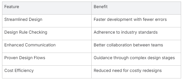
- Streamlined Design Process: PDKs provide essential design guides and tools for engineers. These resources help streamline the design process, reducing time and errors.
- Design Rule Checking: PDKs include design rule checking decks. These ensure that the design follows the necessary rules and standards. This step minimizes costly errors during production.
- Improved Communication: PDKs enable clear communication between foundries and design teams. By having a common set of standards, both parties can better collaborate.
- Enhanced Design Flows: With a PDK, designers have access to proven design flows. These are predefined paths that guide them through the design stages efficiently.
- Cost Efficiency: Using PDKs can lower manufacturing costs. They help ensure that prototypes are accurate, reducing the need for rework.

In summary, PDKs are crucial for ensuring efficient, cost-effective, and error-free semiconductor design.
Significance for ASIC Design Engineers
A Process Design Kit (PDK) is vital in semiconductor design. For design engineers, it serves as a key resource. PDKs provide the design rules and guides needed to create integrated circuits. These kits streamline the design process by offering design tools tailored for specific technologies.
Here’s why PDKs matter to design engineers:
- Design Rules: PDKs contain design rule checking decks. These ensure that designs meet manufacturing requirements.
- Efficiency: Using a PDK speeds up the design flows. It means fewer errors and faster time to market.
- Standardization: PDKs offer consistency. They align with industry standards, making collaboration easier.
- Innovation: With design guides, engineers can focus more on creativity. They don’t have to worry as much about basic compliance.
- Comprehensive Tools: These kits include simulation models and parameterized cells (PCells). These tools help in precise circuit design.
In summary, process design kits are crucial for the semiconductor industry. They assist engineers in overcoming design challenges, leading to efficient and reliable integrated circuit production.
Conclusion: The Future of PDKs in Semiconductor Design
In the semiconductor industry, Process Design Kits (PDKs) are essential. They play a vital role in developing integrated circuits. PDKs streamline the design process by providing design rules, design guides, and design tools. These resources ensure designers can efficiently create robust semiconductor designs.
Future Trends of PDKs:
- Advanced Design Tools: As technology evolves, PDKs will incorporate more sophisticated design tools. This will improve accuracy and speed in the design flows.
- AI Integration: Artificial intelligence may be used to automate design rule checking decks. This will reduce human errors and enhance efficiency.
- Customization: PDKs could offer more customizable options to meet the diverse needs of different semiconductor design projects.
In conclusion, the future of PDKs in semiconductor design looks promising. With continuous innovation, they will become even more integral in producing cutting-edge semiconductor technologies. As designers face new challenges, the evolution of PDKs will be key to overcoming them.
Process Design Kit (PDK) FAQ
What is a Process Design Kit (PDK)?
A Process Design Kit (PDK) is a collection of files and documentation provided by a semiconductor foundry that enables the design and verification of integrated circuits (ICs) for a specific manufacturing process. It acts as a bridge between the design team and the foundry, ensuring that the designed circuit is manufacturable and meets the required performance specifications.
Why is a PDK important for IC design?
A PDK is crucial for IC design as it provides essential information and tools for:
- Device Creation: PDKs include primitive devices (transistors, resistors, capacitors) and models, allowing designers to build circuits at the schematic level and perform simulations.
- Layout Design: PDKs contain design rules (DRC), electrical rules (ERC), and layout versus schematic (LVS) checks to ensure the layout meets manufacturability standards and matches the intended schematic.
- Physical Verification: PDKs offer tools for parasitic extraction, reliability analysis (e.g., electromigration), and sign-off checks to validate the final design before sending it to the foundry.
- Foundry Compatibility: Using the foundry-provided PDK guarantees that the design adheres to the specific process technology and design rules of that foundry, increasing the likelihood of successful fabrication.
What are the key components of a PDK?
A PDK typically includes:
- Technology Files: Define the process technology, including layer information, electrical properties, and design rules.
- Device Libraries: Contain parameterized cells (standard cells, IO cells, memories) and their associated symbols, models, and layout views.
- Design Rule Decks: Specify the geometric and electrical constraints for the layout to ensure manufacturability and reliability.
- Simulation Models: Provide models for transistors, passive components, and interconnect parasitics for accurate circuit simulation.
- Extraction Decks: Define the rules for extracting parasitic capacitances and resistances from the layout.
- Documentation: Includes a design manual, application notes, and examples to guide designers.
What is the role of DRC in a PDK?
Design Rule Checking (DRC) is a critical part of the PDK. It enforces the foundry’s geometric and electrical constraints, ensuring the layout is manufacturable. DRC helps to detect and prevent:
- Spacing Violations: Ensures minimum spacing between different features to avoid short circuits.
- Width Violations: Verifies that all features meet minimum width requirements for proper patterning.
- Notch Violations: Detects unwanted notches that could weaken the structural integrity of features.
- Antenna Violations: Prevents the accumulation of excessive charge during manufacturing, which could damage transistors.
What is the purpose of LVS in a PDK?
Layout Versus Schematic (LVS) verification is a process that checks if the physical layout accurately reflects the intended schematic design. LVS ensures that:
- Connectivity: All connections in the layout match the schematic.
- Device Recognition: All devices in the layout are recognized correctly and match the schematic’s device types.
- Parameter Matching: Device parameters like width and length in the layout align with the schematic.
A successful LVS check confirms that the layout is a faithful implementation of the schematic, minimizing the risk of functional errors.
What is parasitic extraction, and why is it important?
Parasitic extraction is the process of calculating the unintentional resistance (R), capacitance (C), and inductance (L) values introduced by the physical layout of the circuit. These parasitics can significantly impact circuit performance. Extraction is crucial because:
- Timing Analysis: Parasitics affect signal propagation delays, requiring accurate extraction for timing analysis and optimization.
- Signal Integrity: Parasitics contribute to signal distortion and noise, impacting signal quality.
- Power Consumption: Parasitics can lead to increased power consumption due to leakage currents and signal coupling.
What are the different types of PDKs?
PDKs can be categorized based on:
- Foundry: Each foundry (e.g., TSMC, GlobalFoundries, Samsung) provides PDKs specific to their manufacturing processes.
- Technology Node: PDKs are specific to a particular technology node (e.g., 180nm, 45nm, 7nm), defining the feature sizes and process capabilities.
- Process Type: PDKs can be tailored for different process flavors, such as low power, high performance, or mixed-signal applications.
How are PDKs qualified?
PDK qualification involves a rigorous testing process to ensure its accuracy, reliability, and compatibility with design tools. This includes:
- Device Testing: Verifying the behavior of individual devices through simulations and comparisons with measured data.
- Design Rule Checking (DRC): Running DRC on test layouts to confirm rule accuracy and completeness.
- Layout Versus Schematic (LVS): Ensuring the LVS deck correctly identifies and compares devices and interconnections.
- Extraction Testing: Validating the accuracy of parasitic extraction results using benchmark circuits.
- IP Regression Testing: Checking PDK updates against existing designs to ensure compatibility and identify any potential issues.
![]()
![]()