

RF-SOI is name of a specialized semiconductor process utilized to create certain RF Integrated Circuits for applications like antenna tuners for cellphones and switching devices. Essentially, it is RF version of the SOI technology.
Peregrine Semiconductor initiated the SOI process technology in 1990s for standard 0.5μm CMOS node with sapphire substrate as buried oxide for isolation [1]. SOI technology made its place in the market around 2000s. IBM started to use SOI in high-end “ISTAR” Power PC-AS microprocessor.
SOI technology takes benefit of immunity of latch-up effects and has lower substrate loss, thereby resulting in improved RF-characteristics[2]. RF SOI-processed chips deal with a range of applications, but RF front-end modules in smartphones is their big market. RF-SOI has shown its huge production capacity in RF and millimeter-waves telecommunication applications from one to tens of GHz [3]. Gaming console manufacturers like XBOX 360 PLAYSTATION 3, WII have employed 90 nm power architecture based processors to enhance the user experience. AMD (Advanced Micro-Device) started using this technology in 2001 in its 130 nm single core processor.
Single-device islands that are dielectrically isolated (made of SiO2 or Al2O3) from the substrate beneath them as well as from each other make up SOI CMOS circuits. The transistors are encapsulated in insulator on all sides which is selected based on the application e.g. Alumina is opted for radiation-sensitive, high performance applications, whereas, for reduced short channel effects in microelectronics, silica is used.
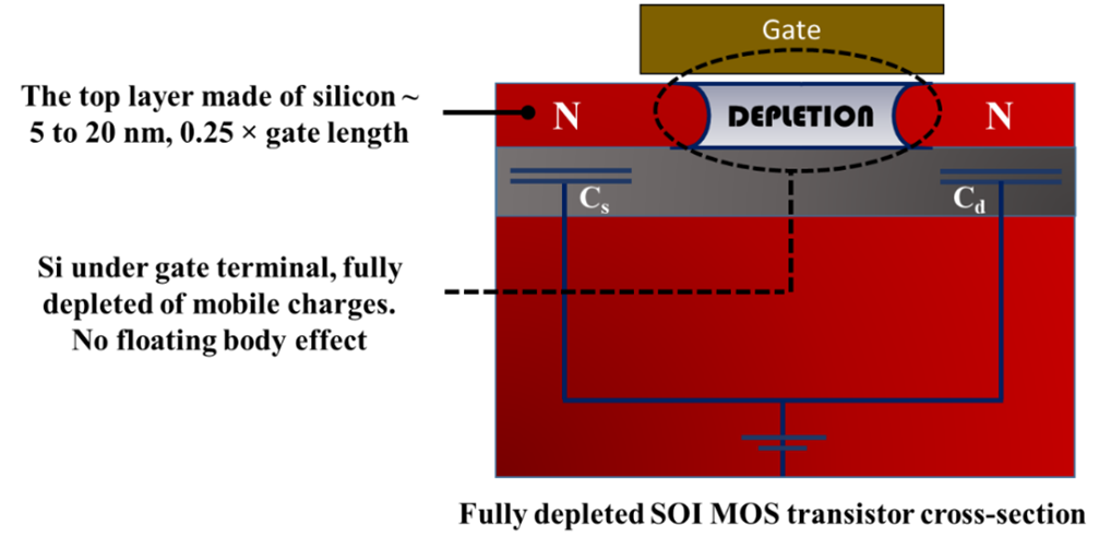
Full Depleted SOI (FDSOI)
In FDSOI, the film is very thin of the order of 5 to 50 nm and the depletion region covers it thoroughly. The thickness of top silicon is kept 5 to 20 nm, the front gate (GOX) is capable of supporting lower number of depleted charges than in the case of bulk devices. Therefore, the inversion charges increase in number resulting in higher switching speeds. For example, in case of NMOS-FET the positive voltage applied to the gate terminal depletes the p-type body, hence inducing the n-type channel inversion on the body surface. This is a lower power consumption technology, meaning lesser heat development such that the FDSOI remains cooler. The thin insulator positioned below channel eliminates need for dopants addition to the channel making it fully depleted. FDSOI has short effective channel length hence has lesser effective time of electrons flow. FDSOI will allow semiconductor industry to deliver next generation digital devices.
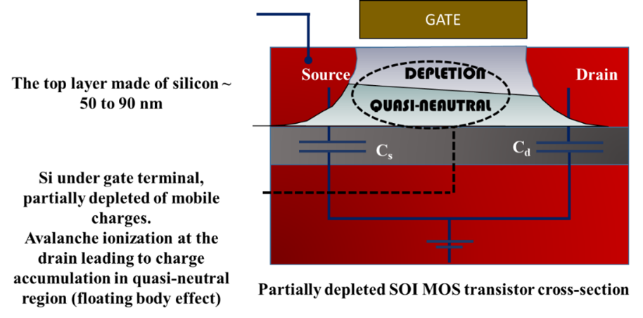
Partially Depleted SOI (PDSOI)
In PDSOI, for the case of NMOS-FET, the p-type film sandwiched between gate as well as buried oxide are large to an extent that the depletion region cannot mask the complete p-region. This attribute makes PDSOI closer to bulk MOSFET. The insulated layer of silicon is not as thin as it is in FDSOI; hence the inversion region is not completely extended over the body. The usual thickness of insulating layer is 100 – 200 nm, with top Si layer of 50 to 90 nm. These chips are used in analog circuits and are relatively easy to manufacture.
Answer a few questions and get a recommended shortlist of foundries. Full scoring and a longer shortlist by email.
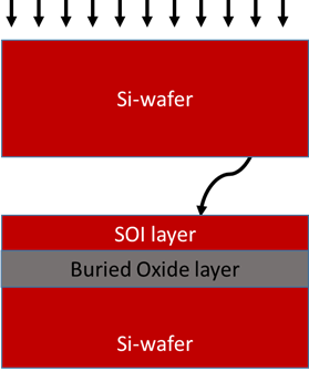
SOI technology refers to using the silicon-insulator-silicon substrate instead of using only silicon.
SOI technology differs from conventional silicon-based devices because of the electrical insulator at silicon junction. SOI chips consume 20% less power and can operate up to 15% quicker than bulk CMOS-based devices. Low noise and high-quality passives are other benefits of SOI involving RF and mixed signals applications. By adding silicide layers, like WSi2, the SOI can be changed to create a Ground Plane Silicon On Insulator (GPSOI), which further improves the decrease of cross-talk[4].
Other benefits over silicon in bulk are as follows:
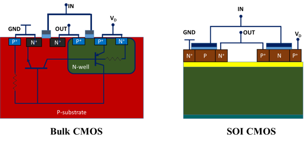
The buried oxide (BOX) in SOI technology allows for vertical isolation from the substrate, which is the most evident distinction between it and bulk methods as shown in Figure below. It is otherwise difficult to preserve the device characteristics when they are brought down to smaller scale, because of the parasitic effects being pronounced. This complete (vertical and lateral) isolation suppresses the substrate coupling processes at low frequencies and avoids the well-known latch-up phenomenon seen in bulk technology by offering low parasitic capacitance[5].
The RF-SOI technology exists in many different topologies as, Silicon on Sapphire (SoS), separation by Implanted Oxygen (SiMoX), bond and etch-back SOI (BESOI), Epitaxial layer transfer (ELTRAN), and smart-cut.
Silicon on Sapphire (SOS)/ Seed method
In this topology, the top silicon is directly grown on insulator. Seed methods necessitates a template for homo-epitaxy. In this format, low channel charge mobility is realized ( 230-250 cm2/Vs)[6].

Separation by Implanted Oxygen (SiMOX)
In this topology, oxygen ions are implanted at higher energies as 120 – 200 keV using a dose of (~0.3 – 1.8) × 1018 cm-2. In this process, the annealing is carried out for longer times as 3 – 6 hours at higher temperatures as 1300° C or above [7]. The typical thickness of 100, 200, 400 nm is realized, where SOI layer is ~50 – 240 nm. The fabrication in SiMOX is two step including “ion implantation” and “annealing”. Oxygen ions are implanted on Si-wafer in implantation step, where they react with Si forming SiO2, which is irregular. The high-temperature annealing repairs the irregularity and make the SiO2 precipitates regular such that the BOX layer becomes efficient [8].
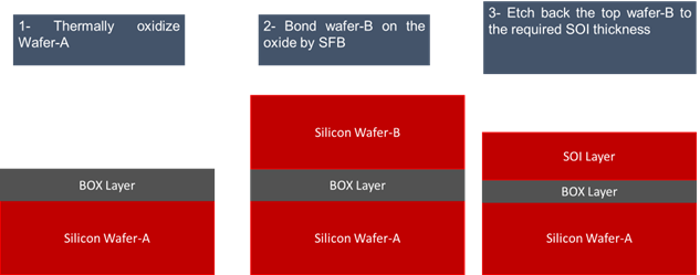
Bond and etch-back SOI (BESOI)
In this method, two Si wafers are tightly bonded with insulator SiO2 layer using the chemical bonding of Si with SiO2 or of SiO2 with SiO2. The bonded SOI wafers are obtained by properly thinning down the bulk Si to a desired thickness. IN BESOI, three steps are involved as shown in the Figure below. First, a non-oxidized wafer is mated at room temperature with a thermally oxidized wafer. Secondly, the bonded pair is annealed for strengthening the bond and thirdly, one of the sides of the bonded pair is thinned down to a desired thickness by grinding, etching and polishing[9].
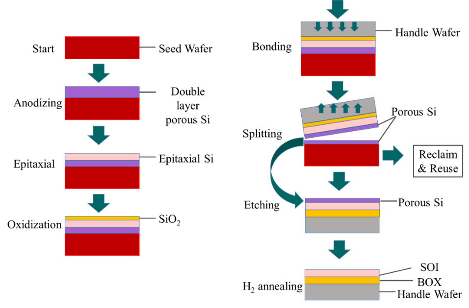
Epitaxial layer transfer (ELTRAN)
ELTRAN is another SOI wafers manufacturing method originally developed by Canon[10]. Wafer bonding and etching porous Si result in the formation of ELTRAN wafers, which are essentially BESOI wafers. The active Si layer is grown epitaxially on porous silicon in a seed wafer during the process’s initial iteration, and the device wafer’s etch-back depends on the porous silicon’s extraordinarily high etch rate. To facilitate the repurposing of the seed wafer by transferring the epitaxial layer onto the handle silicon wafer, a later process of mechanical splitting is included at the porous silicon layer. A basic description of the ELTRAN procedure is given below in the Figure.
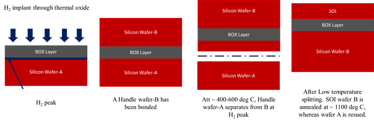
Smart-cut
In this method, Hydrogen dose of > 5×1016 cm-2 is used in order for splitting silicon. The SOI structures are manufactured through implantation of the surface to another wafer. The technology makes use of pressure of hydrogen as a function of temperature and material type, that accumulates in micro-cavities and micro-cracks induced through initial implantation along implanted zone. The thickness of SOI film is subject to H2 implantation energy and BOX layer thickness. The net result is that a thin Si layer, governed by the implant depth [11].
A thin insulating layer, such as SiO2 in order for SOI to function, separates a thin layer of Si and the Si substrate. This procedure contributes to the reduction of junction capacitance, which raises speed and decreases power consumption.
SOI CMOS technology is a worthwhile option for low voltage RF circuits[12]. This technology employs different substrates to prevent the harmonic distortion, which is realized when the electrical equivalent capacitance and conductance become linear i.e. when they are independent of applied voltage. This is not possible with silicon, which has field-effect i.e. the voltage dependent impedance. The carrier mobility must be high for high-speed applications, along with the reduced energy consumption. III-V materials can offer these favors, but their integration is difficult and cost per chip is higher. Thus, silica and Alumina which are cost-effective alternatives, but they lead to lesser mobility due to dimension mismatch. Therefore, to address all this challenges, SOI substrate is made using bulk Si on which SiO2 is grown on which active silicon film is placed to realize the buried oxide (BOX) where this layer electrically isolates each device from other while simultaneously suppressing the substrate coupling. As shown in Figure, the distinctive characteristic of SOI is the manufacturing of the complete integrated-circuit structure in a thin film of premium silicon on top of an insulating layer. This construction offers benefits in terms of yield and performance.
RF-SOI makes the technology capable of carrying higher currents than the equivalent bulk devices. It is a simpler technology having neither wells nor trenches. It has better dielectric isolation vertically and horizontally, allowing denser fabrication, better radiation tolerance, improved power consumption lower temperature dependency, low drain/ source parasitic capacitances and leakage currents thus higher power efficiency, no latch up or leakage path as can be seen from Figure above, due to absence of well in substrate [13]. It is claimed by IBM that in a given area 30% more electronic devices can be fabricated when compared to bulk devices.
The SOI technology has allowed the reduction in power consumption [14]. SOI allows 23% power savings [15]. Chipmakers have shown a confidence in the power Management industry because of SOI technology.
Advantages of SOI CMOS technology include complete integration potential, RF circuits, passive components, and active devices. RF-SOI has allowed the miniaturization of the MOSFET technology[16]. The most exciting feature of this technology is its compatibility with conventional fabrication processes. The ability to combine high-voltage and low-voltage components on a single chip, cost and space savings, streamlined designs and models, and improved performance are some of the possible advantages of SOI. These advantages could reduce development costs and accelerate the market[17].
The SOI technology offers characteristic benefit for analog and RF applications[14]. The benefit of employing highly resistive (insulating) substrate enables mixed-signal applications. RF-SOI has enabled the design of advanced RF front-end modules, RF chips for smartphones, antenna tuners for enhanced reception, WiFi for switch and reception functionalities. In addition, Bellew et al. have reported the SOI procedure for a large series-connection of PV cells[18]. Micro-electro-mechanical systems (MEMS) applications are a focus of the SOI technique, which could connect up to 200 PV cells.
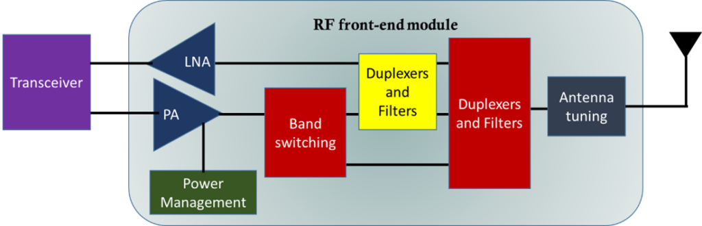
The RF has several bands for wireless systems. RF-SOI has enabled use of these bands of wireless networks for multiple frequencies. Such a circuit is complex, has large number of components and need compatible switches for different frequencies in smartphones. The front-end module (FEM) of a smartphone behaves as an interconnect between RF transceiver and antenna, which is configured by the integration of different components as power amplifiers, antenna tuners, filters, LNAs and RF switches. RF switches are RF SOI chips integrated in smartphones FEM. In addition, the tuners do also have chips based on RF SOI. Signals transportation is accomplished using RF switches, while tuners enable antenna to adjust to any frequency. One of the most intricate and important designs in 4G LTE-A, 5G smartphones and the base-station is the RF FEM. Increasing 5G FEM complexity and integration has resulted in an increase in RF Si content in the newest RF infrastructures and smartphones for multiple antenna elements (or high order MIMO) and many bands along with carrier aggregation requirements.
The importance of IoT has grown over the past several years due to the quick increase in computing devices and data quantities. With trillions of sensors installations, the IoT is poised to transform the world, posing sustainability issues on economic and environmental level due to the carbon footprint associated with sensor nodes, and on the electrical power viz. needed to support the internet traffic. These high-end challenges are being addressed using CMOS technology scaling which reduces the operation to very low-voltage[15].
The well-known device known as radar uses electromagnetic waves to measure, identify, and locate obstacles in the surrounding area. The development of driverless vehicles and advanced driver assistance systems (ADAS) is greatly facilitated by automotive radar. Modern CMOS technology is considered as a prerequisite for meeting the needs of the next generation of radar systems. Radar systems-on-chip (SoC) are transceivers that are fully integrated into a single chip, and they are made feasible by the large increase in integration density that CMOS technology provides. FD-SOI is one of the most promising silicon technologies which has made integration of high-frequency radar components on a single chip possible for automotive radar [19]. The technology has enabled low-power operation and has enhanced radar system performance.
Silicon photonics has gained huge attention in the data-/ tele-com in the recent decades. Numerous integrated photonic active and passive devices have been realized owing to remarkable optical properties of Si in the mid-infrared spectrum. Such devices use high optical constant’ contrast for achieving waveguides on SOI. Excessively increasing traffic in data center, high-performing computer, and telecom sectors requires high-speed, wide-bandwidth, low-cost, and high energy-efficiency data flow which requires the integration of photonics and electronics for extremely quick data transfer in networks [20].
This reduction is size, however, has raised the challenges for every new generation of technology. One of the examples is the leakage current, which due to smaller size of transistors representing a significant part of its power consumption. Another drawback of SOI technology is higher manufacturing costs when compared to the traditional semiconductor methods. Some other drawbacks associated with SOI technology include:
History Effect
In PDSOI, floating body undergoes charging/ discharging leading to change the threshold voltage of MOS transistor due to differences in the floating body voltage. This may change the circuit delay and cause mismatch between two alike devices. The transistors could possess floating body at different voltages according to their prior steady-state condition. They can switch at different instances, depending on accumulated charge. This is known as “History effect”.
Kink Effect
Insulating substrate beneath leads transistor’s body to act as a capacitor upon which charge accumulation takes place which may cause adversarial effects as off-state leakages. The current flowing through the device will be affected, according to the charges accumulated on the floating body. This effect is known as “floating body effect/ Kink effect”.
Self-Healing Effect
The source, body and drain regions are insulated from substrate in SOI. The body is typically unconnected which resulting in a floating body which can get freely charged/ discharged owing to the transients thereby affecting the threshold voltage (Vt) and other device characteristics. The performance, long-term reliability and nonuniform power distribution is caused by the self-heating effect [21]. The self-heating effect of a high-performance circuit built using SOI technology is significantly high.
The main obstacle to SOI implementation is the sharp rise in substrate costs, which adds between 10% and 15% to the overall cost of production. FD-SOI offers the lowest cost per transistor of all CMOS technologies in addition to notable improvements in battery life, or even battery-less solutions. Higher packing density and a smaller “defect susceptible” area are two benefits of SOI material, which translate into increased yield and less final IC costs [22].
The thermal effects of scaled technology and self-heating effect lowers the gate oxide time-to-breakdown. FD-SOI technology has a larger self-heating impact and requires a careful thermal management. Thermal management issue has sheer magnitude for the case of major electronic components; especially transistors where the thermal transfer become increasingly complex at the nanoscale needing extensive care. Almost all performance metrics, like power dissipation/ consumption, speed, device longevity, and cost, are directly impacted by a device’s temperature [23]. Heat affects every part of the finished product and can be measured in terms of decreased processor lifetime or speed. The integrity of the metal interconnects deteriorates with rising temperatures, eventually causing open- and short-circuit failures. Owing to the continuous shrinkage in size and rise in transistor density within a processor, we can generally define four packaging levels in the field of thermal management: (1) the chip/module-level, (2) the board-level, (3) the system-level, and (4) the more recently established transistor-level.
ST, a well renowned company, has created a comprehensive RF-SOI technology portfolio, including the H9SOIFEM and C65SOIFEM nodes, by utilizing its significant expertise in SOI technology. 4G LTE-Advanced and 5G sub-6 GHz RF FEMs with an emphasis on RF integration and switch performance are the main applications of H9SOIFEM technology. The needs of RF FEMs for 2.4 to 5 GHz and narrowband IoT devices are likewise met by H9SOIFEM technology. H9SOIFEM process is produced on an 8-inch wafer, viz. based on a 130 nm technology node.
With the crucial addition of switch capability, C65SOIFEM is tuned for LNA performance throughout the whole 5G sub-6 GHz spectrum. Based on a 65nm technology node, the C65SOIFEM process is produced on 12-inch wafers. It has a 1.2 V MOS that is high-speed and low-noise, with an fMAX of 200 GHz, and is tuned for the 5G sub-6 GHz range.
As with the technology advancements, the sizes of CMOS chips are scaling down and their fabrication needs careful attention to avoid the possible changes in their characteristics, because the parasitic effects are pronounced at micro-scale. It shows promise for various RF and millimeter-wave functional blocks in the direction of full SOI FEM integration.
RFCMOS on SOI is a quickly evolved technology for switches in wireless applications. The RFCMOS-SOI roadmap has been pushed by the need for improved linearity, isolation, and lower insertion loss. The Ron.Coff is a figure-of-merit for RF switching applications and it has decreased from more than 300 fps to less than 200 fps. The switching performance is measured by taking the product of the transistor’s Ron and Coff thus both impacting on the device performance, thus both should be as low as feasible.
SOI implement high-speed ICs for low-power applications. SOI has developed strong footings in semiconductor fabrication industry owing to the associated benefits. A comparison is established on two criteria i.e. average power consumption and circuit speed, for DSP processor chip from a 0.6 µm “bulk CMOS” to a 0.5 µm “SOI CMOS” technology in [24]. It is found that the SOI circuit operated at 98 MHz speed, which is 51% higher than that of the original i.e. 65 MHz. In addition, the average power consumption is 35% lesser in SOI circuit when 3.3V, 35 MHz source was used for bulk and SOI CMOS designs.
In both bulk and SOI CMOS devices, gate capacitance is the predominant. In SOI these junction/ parasitic capacitances are diminished by a factor of four to seven due to being isolated dielectrically. Low power, fast speed, high device density, and the floating body effect are the exceptional qualities of SOI [25]. Additionally, the device topology enhances soft error immunity, short channel effect, and eliminates the latch up in bulk CMOS. Nevertheless, despite these benefits, the SOI technology still has to overcome some significant obstacles, including concerns with circuit design, manufacturing availability, and process availability. The technology is not yet advanced enough to produce low-cost, low-defect-density substrates in large quantities [25].
One of the main issues in highly integrated RF/mixed mode circuit design is the prevention of digital, mixed signal devices on the same chip from talking to high frequency RF. The design benefit of SOI CMOS includes a notable decrease in crosstalk between digital circuits and RF on the same chip and simple integration of premium passive components [26]. Due to the inherent faster speed, gallium arsenide (GaAs) has been employed widely in RF applications operating in the 2 to 6 GHz range, but so far as cost of integration is concerned, CMOS technology is better choice. The fact prevails more in advanced CMOS technology, as a 2.4 GHz transceiver has been demonstrated for Bluetooth application with a deep sub-micron CMOS technology [27] which is faster than 900 MHz Industrial, Scientific and Medical (ISM) band transceivers.
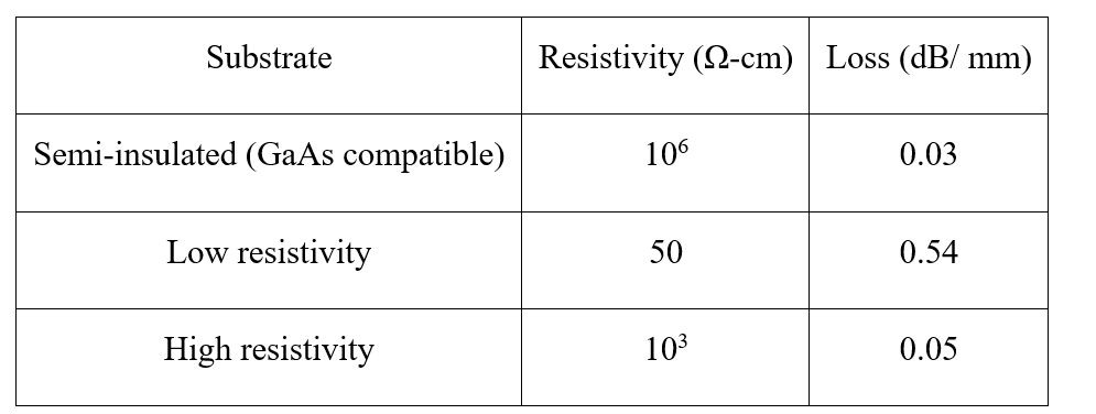
Due to the short battery life of mobile devices, low power consumption is very crucial. One way to overcome this difficulty is to develop a low-power RF system-on-a-chip that integrates the digital, analogue, and RF components onto a single die where SOI CMOS satisfies these requirements due to lower parasitic capacitance. In addition, BOX allows for the flexible use of a high resistivity substrate to lower substrate-related RF losses. On high resistivity substrates, microstrip losses as little as 0.03 dB/mm have been achieved at 2 GHz, in contrast to 0.1 dB/mm on normal substrates as given in Table 1 [26]. Furthermore, enhanced passive device performance with frequency has also been reported on SOI substrates [26].
Table 1. Microstrip loss reduction through high resistivity SOI substrate
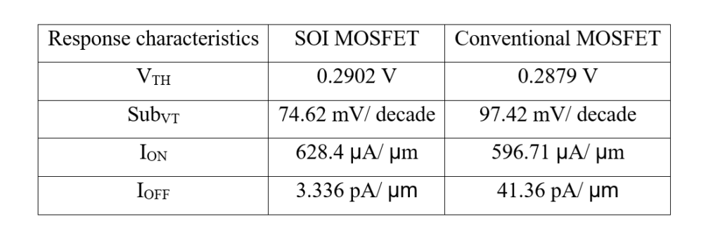
Conventional MOSFETs have already achieved transistor production capabilities below 45 nm. Nowadays, silicon is approaching atomic resolution and its physical and electrical limits, making the process of creating a functional transistor increasingly challenging and complex. The main task is to create a transistor with reduced drain induced barrier lowering (DIBL), lower gate leakage current (IOFF), and nominal threshold voltage (VTH). The SOI MOSFET has presented a solution to these issues, and it is thought to be able to suppress SCEs by burying an oxide-layer in si substrate. In [28], once more, it is proven that the overall electrical characteristics of the SOI MOSFET were better than those of the traditional MOSFET, as given in Table2, drawn after reuse from [28].
Table 2. SOI and Bulk MOSFET electrical characteristics Comparison
The SOI is the future of RF technology as it is characterized with reduced junction capacitance, it is free from latchup, has ease in scaling as BOX does not need scaling, compatible with conventional silicon processing, it has reduced leakage.
It is projected that the global market for RF SOI & SOS switches will grow significantly between 2023 and 2030. Amidst the overwhelming demand for this technology for smartphones, foundries are increasing their fab capabilities for RF SOI procedures as the RFSOI battle has begun. They are expanding their 200mm RF SOI fab capacities in order to keep up with the rapidly rising demand. In a seemingly competitive to secure the initial wave of RF business for 5G, the upcoming wireless standard, GlobalFoundries, TowerJazz, TSMC, and UMC are growing or initiating RFSOI processes in 300mm fabs. 300mm provides full automation, process control and integration. RF SOI wafer shipments have reached to 1.6 million in total in 2018, which is expected to surpass two million soon [29].
[1] A. K. Agarwal et al., “Microx – An All Silicon Microwave Technology,” in 1992 IEEE International SOI Conference, 1992, pp. 144–145. doi: 10.1109/SOI.1992.664833.
[2] R. F. P. S. Vdmosfets et al., “RF Power Silicon-On-Glass VDMOSFETs ´ ,” IEEE Electron Device Letters, vol. 25, no. 6. pp. 424–426, 2004.
[3] M. Rack and J.-P. Raskin, “SOI Technologies for RF and Millimeter-Wave Applications,” Convergence of More Moore, More Than Moore, and Beyond Moore. pp. 131–182, 2020. doi: 10.1201/9781003043034-5.
[4] “Silicon On Insulator (SOI) | Queen’s Advanced MicroEngineering Centre.” https://www.qub.ac.uk/research-centres/QAMEC/ResearchActivities/SiliconOnInsulatorSOI/#:~:text=SOI works by placing a,speed and lower power consumption. (accessed Nov. 26, 2023).
[5] J.-L. Leray, “Chapter 2 A review of buried oxide structures and SOI technologies,” in New Insulators, Devices and Radiation Effects, vol. 3, G. Barbottin and A. B. T.-I. in S. D. Vapaille, Eds. North-Holland, 1999, pp. 145–231. doi: https://doi.org/10.1016/S1874-5903(99)80008-1.
[6] “Silicon on Insulator Technology,” The VLSI Handbook. pp. 109–124, 2020. doi: 10.1201/9781420049671-5.
[7] “US5888297A – Method of fabricating SOI substrate – Google Patents.” https://patents.google.com/patent/US5888297 (accessed Nov. 16, 2023).
[8] I. Hamaguchi, T. Yano, K. Kajiyama, and S. I. Hayashi, “Dislocation density reduction in simox (Separation by implanted oxygen) multi-energy single implantation,” Japanese Journal of Applied Physics, vol. 34, no. 6R. pp. 2989–2993, 1995. doi: 10.1143/JJAP.34.2989.
[9] H. Baumgart, T. J. Letavic, and R. Egloff, “Evaluation of wafer bonding and etch back for SOI technology,” Philips Journal of Research, vol. 49, no. 1–2. pp. 91–124, 1995. doi: 10.1016/0165-5817(95)82005-1.
[10] K. Sakaguchii, “Current progress in epitaxial layer transfer eltran,” IEICE Transactions on Electronics, vol. E80-C, no. 3. pp. 378–386, 1997.
[11] J.-P. Colinge, “Silicon-on-Insulator and Porous Silicon BT – Silicon: Evolution and Future of a Technology,” P. Siffert and E. F. Krimmel, Eds. Berlin, Heidelberg: Springer Berlin Heidelberg, 2004, pp. 139–167. doi: 10.1007/978-3-662-09897-4_8.
[12] R. Huang, H. Liao, and G. Zhang, “SOI CMOS technology for RF/MMIC applications – yes or no?,” in Proceedings of 35th European Solid-State Device Research Conference, 2005. ESSDERC 2005., 2005, pp. 241–244. doi: 10.1109/ESSDER.2005.1546630.
[13] X. Li, Q. Liu, S. Pang, K. Xu, H. Tang, and C. Sun, “High-temperature piezoresistive pressure sensor based on implantation of oxygen into silicon wafer,” Sensors Actuators A Phys., vol. 179, pp. 277–282, 2012, doi: https://doi.org/10.1016/j.sna.2012.03.027.
[14] O. Rozeau, J. Jomaah, S. Haendler, J. Boussey, and F. Balestra, “SOI Technologies Overview for Low-Power Low-Voltage Radio-Frequency Applications,” Analog Integr. Circuits Signal Process., vol. 25, no. 2, pp. 93–114, 2000, doi: 10.1023/A:1008376514991.
[15] D. Bol, G. de Streel, and D. Flandre, “Can we connect trillions of IoT sensors in a sustainable way? A technology/circuit perspective (Invited),” in 2015 IEEE SOI-3D-Subthreshold Microelectronics Technology Unified Conference (S3S), 2015, pp. 1–3. doi: 10.1109/S3S.2015.7333500.
[16] S. Cristoloveanu, “From SOI Basics to Nano-Size MOSFETs.” pp. 67–104, 2007. doi: 10.1007/978-0-387-49965-9_2.
[17] J. M. C. Stork and G. P. Hosey, “SOI technology for power management in automotive and industrial applications,” Solid. State. Electron., vol. 128, pp. 3–9, 2017, doi: https://doi.org/10.1016/j.sse.2016.10.033.
[18] C. L. Bellew, S. Hollar, and K. S. J. Pister, “An SOI process for fabrication of solar cells, transistors and electrostatic actuators,” TRANSDUCERS 2003 – 12th International Conference on Solid-State Sensors, Actuators and Microsystems, Digest of Technical Papers, vol. 2. pp. 1075–1079, 2003. doi: 10.1109/SENSOR.2003.1216955.
[19] “Bosch to use FD-SOI for automotive radar SoCs.” https://www.electronicsweekly.com/news/business/bosch-use-fd-soi-automotive-radar-socs-2021-03/ (accessed Nov. 21, 2023).
[20] F. Testa, A. Bianchi, S. Stracca, and R. Sabella, “Silicon photonics for telecom and datacom applications,” Topics in Applied Physics, vol. 122. pp. 421–446, 2016. doi: 10.1007/978-3-642-10503-6_15.
[21] O. Semenov, A. Vassighi, and M. Sachdev, “Impact of self-heating effect on long-term reliability and performance degradation in CMOS circuits,” IEEE Trans. Device Mater. Reliab., vol. 6, no. 1, pp. 17–27, 2006, doi: 10.1109/TDMR.2006.870340.
[22] N. Sugii, “Silicon-on-insulator (SOI) complementary metal oxide semiconductor (CMOS) circuits for ultralow power (ULP) applications,” Silicon-On-Insulator (SOI) Technology: Manufacture and Applications. pp. 318–357, 2014. doi: 10.1533/9780857099259.2.318.
[23] S. Reda, R. Cochran, and A. N. Nowroz, “Improved thermal tracking for processors using hard and soft sensor allocation techniques,” IEEE Transactions on Computers, vol. 60, no. 6. pp. 841–851, 2011. doi: 10.1109/TC.2011.45.
[24] P. Simonen, A. Heinonen, M. Kuulusa, and J. Nurmi, “Comparison of bulk and SOI CMOS technologies in a DSP processor circuit implementation,” Proceedings of the International Conference on Microelectronics, ICM, vol. 2001-Janua. pp. 107–110, 2001. doi: 10.1109/ICM.2001.997499.
[25] V. Ma, “SOI vs CMOS for Analog Circuit.” p. 16, 2001. [Online]. Available: http://www.eecg.toronto.edu/~kphang/papers/2001/ma_SOI.pdf
[26] J. Yue and J. Kriz, “SOI CMOS technology for RF system-on-chip applications,” Microwave Journal, vol. 45, no. 1. 2002.
[27] H. Darabi et al., “A 2.4-GHz CMOS transceiver for Bluetooth,” IEEE J. Solid-State Circuits, vol. 36, no. 12, pp. 2016–2024, 2001, doi: 10.1109/4.972152.
[28] M. N. I. A. Aziz, F. Salehuddin, A. S. M. Zain, K. E. Kaharudin, and S. A. Radzi, “Comparison of electrical characteristics between Bulk MOSFET and Silicon-on-insulator (SOI) MOSFET,” Journal of Telecommunication, Electronic and Computer Engineering, vol. 6, no. 2. pp. 45–49, 2014.
[29] “A review of buried oxide structures and SOI technologies.”
